semi合集-English.pdf - 第7442页
K V B G O R S Q D H P M A I T U L E J W N F C K V B G OR S Q D H P M A I T U L E J W N F C 715 720 725 730 735 0.0 0.2 0.4 0.6 0.8 1.0 1.2 Repeatability Reproducibility Mean Center Point Thickness, m r and R , m Figu…
X
Y
-100 -50 0 50 100
-100
-50
0
50
100
1 2 3 4 5
6 7 8 9 10 11 12 13 14
15 16 17 18 19 20 21 22 23 24 25
26 27 28 29 30 31 32 33 34 35 36
37 38 39 40 41 42 43 44 45 46 47 48 49
50 51 52 53 54 55 56 57 58 59 60 61 62
63 64 65 66 67 68 69 70 71 72 73 74 75
76 77 78 79 80 81 82 83 84 85 86 87 88
89 90 91 92 93 94 95 96 97 98 99 100 101
102 103 104 105 106 107 108 109 110 111 112
113 114 115 116 117 118 119 120 121 122 123
124 125 126 127 128 129 130 131 132
133 134 135 136 137
Wed Jun 30 09:30:04 1999
siteX = 15 siteY = 15 Diam = 200 Edge Excl. = 3 X-off = 0 Y-off = 0
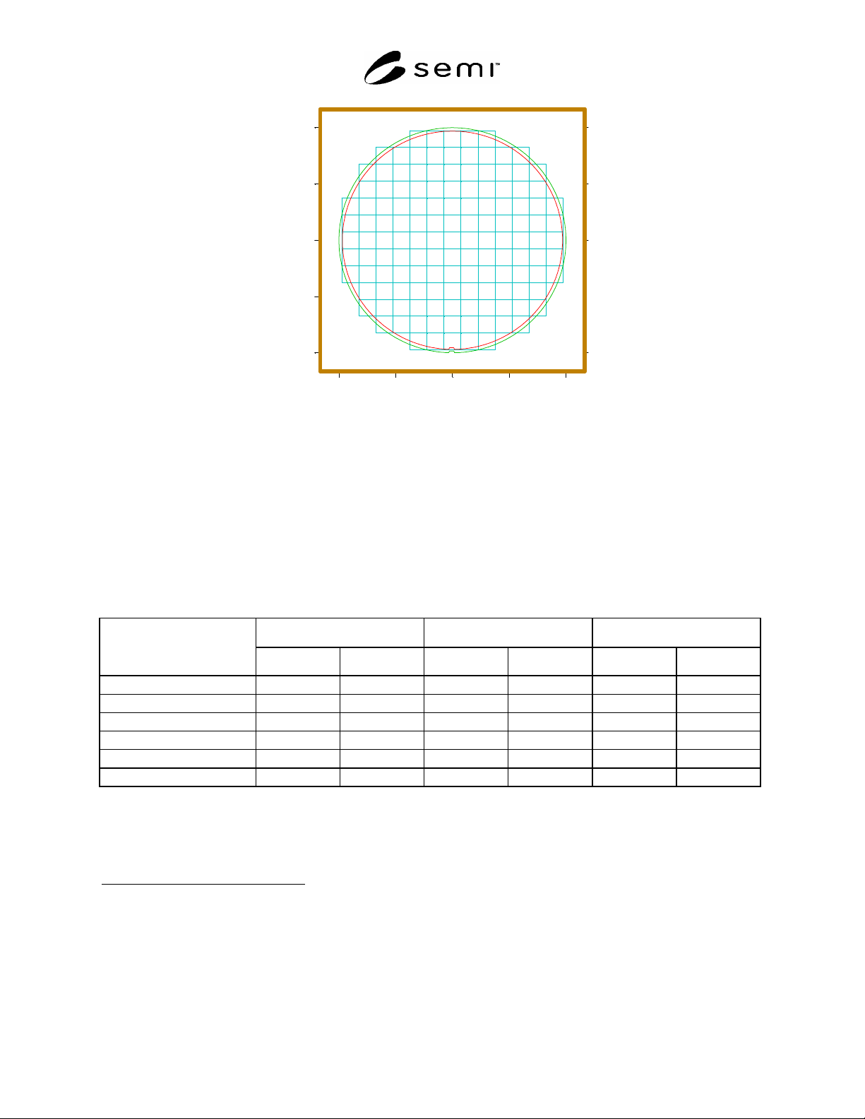
Figure 2
15 mm by 15 mm Site Array on 200 mm Wafer with 3 mm Nominal Edge Exclusion
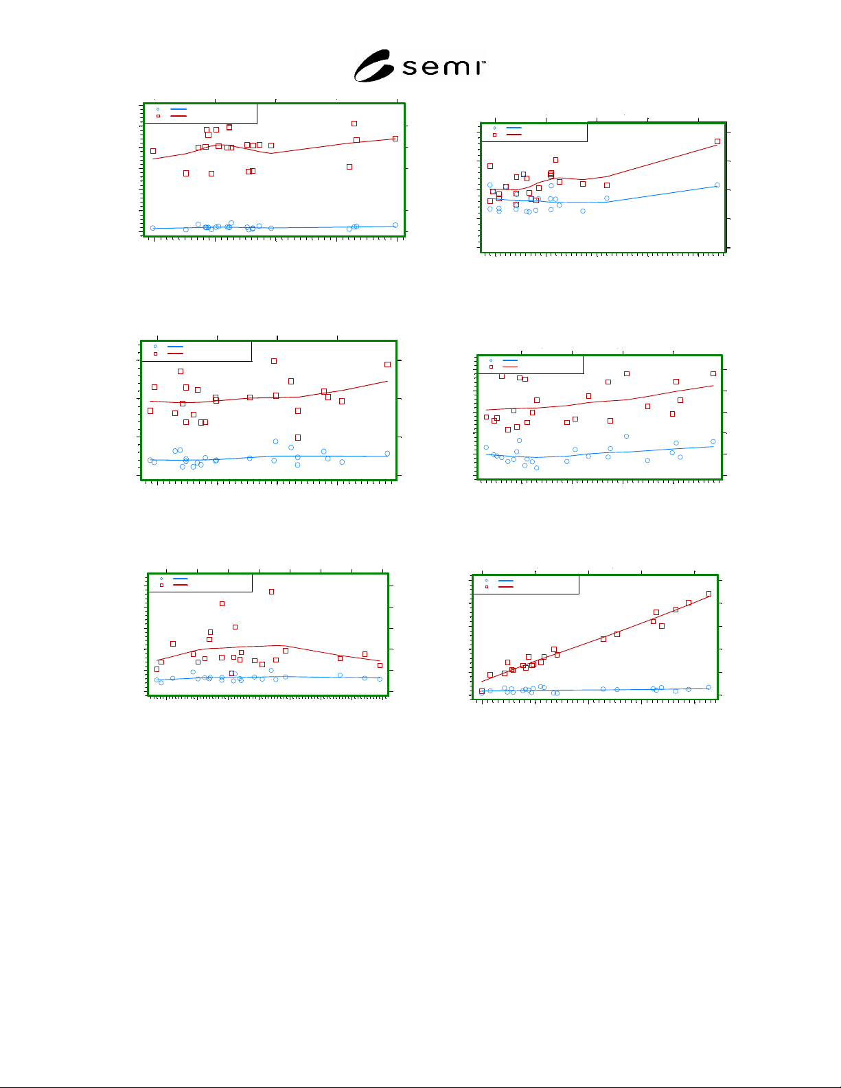
15.7 Figures 3 through 8 contain plots of repeatability (r) and reproducibility (R) for the various parameters: center-
point thickness and TTV for the wafers, and SBIR for the four analyzed sites against mean value.
15.8 For more details, refer to the Research Report.
2
16 Keywords
flatness; noncontact measurement; semiconductor; silicon; thickness; thickness variation; wafers
Table 3 Summary Measurement Statistics
Mean,
m r,
m R,
m
Parameter
Smallest Largest Smallest Largest Smallest Largest
Center Point Thickness 714.86 735.87 0.028 0.085 0.563 1.039
TTV 0.94 2.39 0.026 0.091 0.100 0.292
SBIR Site 069 0.09 0.24 0.010 0.012 0.017 0.095
SBIR Site 073 0.14 0.54 0.013 0.026 0.015 0.037
SBIR Site 075 0.29 1.16 0.017 0.093 0.109 0.243
SBIR Site 135 0.20 1.05 0.015 0.068 0.035 0.892
2 Available on request from SEMI Headquarters, Publications Department, 3081 Zanker Road, San Jose, CA, Fax: 408-943-7015. Request
International Standards Research Report F01–1016, ASTM Interlaboratory Round Robin Experiment on Measuring Warp on Silicon Wafers by
Automated Noncontact Scanning and Measuring Flatness, Thickness and Thickness Variation of Silicon Wafers by Automated Noncontact
Scanning.
SEMI MF1530-1104 © SEMI 2003, 2004 7
K
V
B
G
O
R
S
Q
D
H
P
M
A
I
T
U
L
E
J
W
N
F
C
K
V
B
G
OR
S
Q
D
H
P
M
A
I
T
U
L
E
J
W
N
F
C
715 720 725 730 735
0.0
0.2
0.4
0.6
0.8
1.0
1.2
Repeatability
Reproducibility
Mean Center Point Thickness, m
r and R,
m
Figure 3
Center Point Thickness Repeatability &
Reproducibility
Mean TTV,
m
r and R,
m
F
W
E
V
S
A
B
K
H
T
G
C
D
O
I
N
M
U
R
J
L
Q
P
F
W
E
V
S
A
B
K
H
T
G
C
D
O
I
N
M
U
R
J
L
Q
P
1.0 1.5 2.0 2.5
0.0
0.1
0.2
0.3
Repeatability
Reproducibility
Figure 4
TTV Repeatability & Reproducibility
Site 69 Mean SBIR, m
r and R,
m
W
V
D
F
H
K
A
B
R
E
G
T
P
I
S
L
M
N
U
C
J
O
Q
W
V
D
F
H
K
A
B
R
E
G
T
P
I
S
L
M
N
U
C
J
O
Q
0.10 0.12 0.14 0.16 0.18 0.20 0.22 0.24
0.0
0.02
0.04
0.06
0.08
0.10
Repeatability
Reproducibility
Figure 5
Site 69 SBIR Repeatability & Reproducibility
Site 73 Mean SBIR, m
r and R,
m
G
H
F
S
T
R
W
A
Q
C
M
K
D
U
E
O
N
B
I
V
J
L
P
G
H
F
S
T
R
W
A
Q
C
M
K
D
U
E
O
N
B
I
V
J
L
P
pp
0.1 0.2 0.3 0.4 0.5
0.0
0.01
0.02
0.03
0.04
Repeatability
Reproducibility
Figure 6
Site 73 SBIR Repeatability & Reproducibility
Site 75 Mean SBIR,
m
r and R,
m
K
G
F
V
B
E
A
O
T
C
D
S
H
I
W
U
L
P
R
J
N
Q
M
K
G
F
V
B
E
A
O
T
C
D
S
H
I
W
U
L
P
R
J
N
Q
M
pp
0.4
0.6
0.8
1.0
0.0
0.05
0.10
0.15
0.20
0.25
Repeatability
Reproducibility
Figure 7
Site 75 SBIR Repeatability & Reproducibility
Site 135 Mean SBIR, m
r and R,
m
B
K
E
V
F
T
O
G
A
S
H
D
C
W
U
L
J
P
N
I
R
Q
M
B
K
E
V
F
T
O
G
A
S
H
D
C
W
U
L
J
P
N
I
R
Q
M
pp
0.2 0.4 0.6 0.8 1.0
0.0
0.2
0.4
0.6
0.8
1.0
Repeatability
Reproducibility
Figure 8
Site 135 SBIR Repeatability & Reproducibility
NOTICE: SEMI makes no warranties or representations as to the suitability of the standards set forth herein for any
particular application. The determination of the suitability of the standard is solely the responsibility of the user.
Users are cautioned to refer to manufacturer's instructions, product labels, product data sheets, and other relevant
literature, respecting any materials or equipment mentioned herein. These standards are subject to change without
notice.
By publication of this standard, Semiconductor Equipment and Materials International (SEMI) takes no position
respecting the validity of any patent rights or copyrights asserted in connection with any items mentioned in this
standard. Users of this standard are expressly advised that determination of any such patent rights or copyrights, and
the risk of infringement of such rights are entirely their own responsibility.
Copyright by SEMI® (Semiconductor Equipment and Materials
International), 3081 Zanker Road, San Jose, CA 95134. Reproduction of
the contents in whole or in part is forbidden without express written
consent of SEMI.
SEMI MF1530-1104 © SEMI 2003, 2004 8

SEMI MF1535-1104 © SEMI 2004 1
SEMI MF1535-1104
TEST METHOD FOR CARRIER RECOMBINATION LIFETIME IN
SILICON WAFERS BY NON-CONTACT MEASUREMENT OF
PHOTOCONDUCTIVITY DECAY BY MICROWAVE REFLECTANCE
This guide was technically approved by the Global Silicon Wafer Committee and is the direct responsibility
of the North American Silicon Wafer Committee. Current edition approved for publication by the North
American Regional Standards Committee on August 16, 2004. Initially available at www.semi.org
September 2004; to be published November 2004. Original edition published by ASTM International as
ASTM F 1535-94. Last previous edition SEMI MF1535-00.
1 Purpose
1.1 If the free carrier density of a semiconductor is not
too high, the carrier recombination lifetime is controlled
by impurity centers that have energies located in the
forbidden energy gap. Many metallic impurities form
such recombination centers in silicon. In most cases,
very small densities of these impurities (10
10
to 10
13
atoms/cm
3
) reduce the carrier recombination lifetime
and adversely affect device and circuit performance. In
some cases, such as very fast bipolar switching devices
and high power devices, the recombination
characteristics must be carefully controlled to obtain the
desired device performance.
1.2 This test method covers a procedure for measuring
carrier recombination lifetime in a variety of types of
silicon wafers. Because electrical contact is not made
to the wafer during the test, additional processing steps
can be carried out following the test if wafer cleanness
is maintained.
1.3 This test method is suitable for use in research and
development, process control, and materials acceptance
applications. However, because the precision of this
test method has not yet been established by
interlaboratory test, it should be used for materials
specification and acceptance only after the parties to the
test have established reproducibility and correlation.
2 Scope
2.1 This test method covers the measurement of carrier
lifetime appropriate to carrier recombination processes
in homogeneously doped, polished, n- or p-type silicon
wafers with room-temperature resistivity greater than
about 0.05 ·cm. This test method may also be applied
to the measurement of carrier recombination lifetime in
as-cut, lapped, or etched wafers provided that the
sensitivity of the conductivity detection system is
adequate.
2.2 In this test method, the decay of the wafer
conductivity following generation of excess carriers
with a light pulse is determined by monitoring the
microwave reflectivity of the wafer. Since no contact is
made to the specimen, this test method is
nondestructive. If wafer cleanness is maintained,
wafers may be further processed following testing by
this test method.
2.3 Depending on the level of photoexcitation, the
carrier recombination lifetime determined by this test
method may be the minority-carrier lifetime (low
injection level) or a mixture of minority- and majority-
carrier lifetimes (intermediate and high injection
levels). In the latter case, the minority and majority
carrier lifetimes may be separated under some
conditions if a single recombination center that follows
the Shockley-Read-Hall model is assumed (see Related
Information 1).
2.4 This test method is appropriate for the
measurement of carrier recombination lifetimes in the
range from 0.25 s to >1 ms. The shortest measurable
lifetime values are governed by the turn-off
characteristics of the light source and by the sampling
frequency of the decay signal analyzer while the longest
values are determined by the geometry of the test
specimen and the degree of passivation of the wafer
surface. With suitable passivation procedures, such as
thermal oxidation or immersion in a suitable solution,
lifetimes as long as tens of milliseconds can be
determined in polished wafers with thickness as
specified in SEMI M1.
NOTE 1: Carrier recombination lifetime of large bulk
specimens can be determined by Method A or B of SEMI
MF28. These test methods, which are also based on
measurement of photoconductivity decay (PCD), require
electrical contacts to the specimen. In addition, they assume
large surface recombination on all surfaces and so the upper
limit of measurable lifetime is governed by the size of the test
specimen. Method B of SEMI MF28 stipulates that the test
be carried out under conditions of low injection to ensure that
the minority-carrier lifetime is determined. Minority-carrier
lifetime can also be deduced from the carrier diffusion length
as measured by the surface photovoltage (SPV) method in
accordance with Method A or B of SEMI MF391. When
carried out under low injection conditions, both the SPV
method and the PCD method should yield the same values of
minority-carrier lifetime
1
under certain conditions. First, it is
1 Saritas, M., and McKell, H. D., “Comparison of Minority-Carrier
Diffusion Length Measurements in Silicon by the Photoconductive