semi合集-English.pdf - 第7443页
SEMI MF1535-1104 © SEMI 2004 1 SEMI MF1535-1104 TEST METHOD FOR CARRIER RE COMBINATION LIFETIME IN SILICON WAFERS BY NON- CONTACT MEASUREMENT OF PHOTOCONDUCTIVITY DECAY BY MICROWAVE REFLECTANCE This guide was technically…
K
V
B
G
O
R
S
Q
D
H
P
M
A
I
T
U
L
E
J
W
N
F
C
K
V
B
G
OR
S
Q
D
H
P
M
A
I
T
U
L
E
J
W
N
F
C
715 720 725 730 735
0.0
0.2
0.4
0.6
0.8
1.0
1.2
Repeatability
Reproducibility
Mean Center Point Thickness, m
r and R,
m
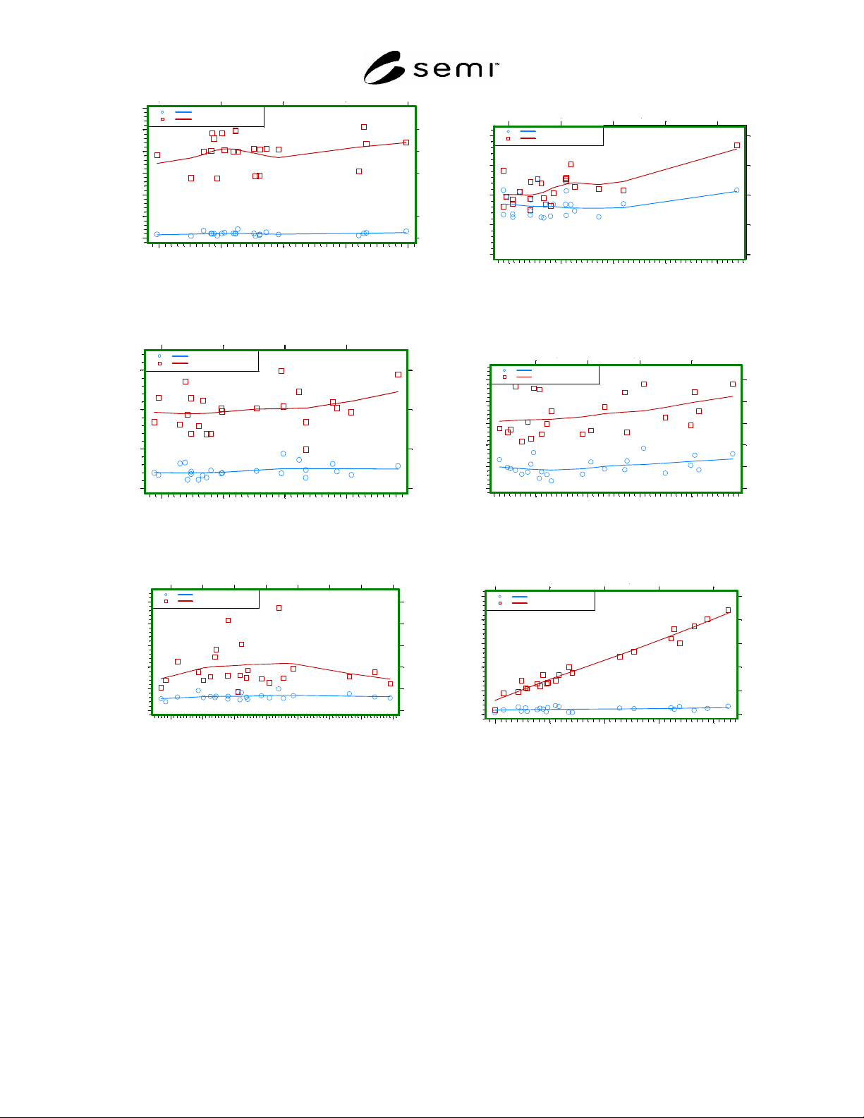
Figure 3
Center Point Thickness Repeatability &
Reproducibility
Mean TTV,
m
r and R,
m
F
W
E
V
S
A
B
K
H
T
G
C
D
O
I
N
M
U
R
J
L
Q
P
F
W
E
V
S
A
B
K
H
T
G
C
D
O
I
N
M
U
R
J
L
Q
P
1.0 1.5 2.0 2.5
0.0
0.1
0.2
0.3
Repeatability
Reproducibility
Figure 4
TTV Repeatability & Reproducibility
Site 69 Mean SBIR, m
r and R,
m
W
V
D
F
H
K
A
B
R
E
G
T
P
I
S
L
M
N
U
C
J
O
Q
W
V
D
F
H
K
A
B
R
E
G
T
P
I
S
L
M
N
U
C
J
O
Q
0.10 0.12 0.14 0.16 0.18 0.20 0.22 0.24
0.0
0.02
0.04
0.06
0.08
0.10
Repeatability
Reproducibility
Figure 5
Site 69 SBIR Repeatability & Reproducibility
Site 73 Mean SBIR, m
r and R,
m
G
H
F
S
T
R
W
A
Q
C
M
K
D
U
E
O
N
B
I
V
J
L
P
G
H
F
S
T
R
W
A
Q
C
M
K
D
U
E
O
N
B
I
V
J
L
P
pp
0.1 0.2 0.3 0.4 0.5
0.0
0.01
0.02
0.03
0.04
Repeatability
Reproducibility
Figure 6
Site 73 SBIR Repeatability & Reproducibility
Site 75 Mean SBIR,
m
r and R,
m
K
G
F
V
B
E
A
O
T
C
D
S
H
I
W
U
L
P
R
J
N
Q
M
K
G
F
V
B
E
A
O
T
C
D
S
H
I
W
U
L
P
R
J
N
Q
M
pp
0.4
0.6
0.8
1.0
0.0
0.05
0.10
0.15
0.20
0.25
Repeatability
Reproducibility
Figure 7
Site 75 SBIR Repeatability & Reproducibility
Site 135 Mean SBIR, m
r and R,
m
B
K
E
V
F
T
O
G
A
S
H
D
C
W
U
L
J
P
N
I
R
Q
M
B
K
E
V
F
T
O
G
A
S
H
D
C
W
U
L
J
P
N
I
R
Q
M
pp
0.2 0.4 0.6 0.8 1.0
0.0
0.2
0.4
0.6
0.8
1.0
Repeatability
Reproducibility
Figure 8
Site 135 SBIR Repeatability & Reproducibility
NOTICE: SEMI makes no warranties or representations as to the suitability of the standards set forth herein for any
particular application. The determination of the suitability of the standard is solely the responsibility of the user.
Users are cautioned to refer to manufacturer's instructions, product labels, product data sheets, and other relevant
literature, respecting any materials or equipment mentioned herein. These standards are subject to change without
notice.
By publication of this standard, Semiconductor Equipment and Materials International (SEMI) takes no position
respecting the validity of any patent rights or copyrights asserted in connection with any items mentioned in this
standard. Users of this standard are expressly advised that determination of any such patent rights or copyrights, and
the risk of infringement of such rights are entirely their own responsibility.
Copyright by SEMI® (Semiconductor Equipment and Materials
International), 3081 Zanker Road, San Jose, CA 95134. Reproduction of
the contents in whole or in part is forbidden without express written
consent of SEMI.
SEMI MF1530-1104 © SEMI 2003, 2004 8

SEMI MF1535-1104 © SEMI 2004 1
SEMI MF1535-1104
TEST METHOD FOR CARRIER RECOMBINATION LIFETIME IN
SILICON WAFERS BY NON-CONTACT MEASUREMENT OF
PHOTOCONDUCTIVITY DECAY BY MICROWAVE REFLECTANCE
This guide was technically approved by the Global Silicon Wafer Committee and is the direct responsibility
of the North American Silicon Wafer Committee. Current edition approved for publication by the North
American Regional Standards Committee on August 16, 2004. Initially available at www.semi.org
September 2004; to be published November 2004. Original edition published by ASTM International as
ASTM F 1535-94. Last previous edition SEMI MF1535-00.
1 Purpose
1.1 If the free carrier density of a semiconductor is not
too high, the carrier recombination lifetime is controlled
by impurity centers that have energies located in the
forbidden energy gap. Many metallic impurities form
such recombination centers in silicon. In most cases,
very small densities of these impurities (10
10
to 10
13
atoms/cm
3
) reduce the carrier recombination lifetime
and adversely affect device and circuit performance. In
some cases, such as very fast bipolar switching devices
and high power devices, the recombination
characteristics must be carefully controlled to obtain the
desired device performance.
1.2 This test method covers a procedure for measuring
carrier recombination lifetime in a variety of types of
silicon wafers. Because electrical contact is not made
to the wafer during the test, additional processing steps
can be carried out following the test if wafer cleanness
is maintained.
1.3 This test method is suitable for use in research and
development, process control, and materials acceptance
applications. However, because the precision of this
test method has not yet been established by
interlaboratory test, it should be used for materials
specification and acceptance only after the parties to the
test have established reproducibility and correlation.
2 Scope
2.1 This test method covers the measurement of carrier
lifetime appropriate to carrier recombination processes
in homogeneously doped, polished, n- or p-type silicon
wafers with room-temperature resistivity greater than
about 0.05 ·cm. This test method may also be applied
to the measurement of carrier recombination lifetime in
as-cut, lapped, or etched wafers provided that the
sensitivity of the conductivity detection system is
adequate.
2.2 In this test method, the decay of the wafer
conductivity following generation of excess carriers
with a light pulse is determined by monitoring the
microwave reflectivity of the wafer. Since no contact is
made to the specimen, this test method is
nondestructive. If wafer cleanness is maintained,
wafers may be further processed following testing by
this test method.
2.3 Depending on the level of photoexcitation, the
carrier recombination lifetime determined by this test
method may be the minority-carrier lifetime (low
injection level) or a mixture of minority- and majority-
carrier lifetimes (intermediate and high injection
levels). In the latter case, the minority and majority
carrier lifetimes may be separated under some
conditions if a single recombination center that follows
the Shockley-Read-Hall model is assumed (see Related
Information 1).
2.4 This test method is appropriate for the
measurement of carrier recombination lifetimes in the
range from 0.25 s to >1 ms. The shortest measurable
lifetime values are governed by the turn-off
characteristics of the light source and by the sampling
frequency of the decay signal analyzer while the longest
values are determined by the geometry of the test
specimen and the degree of passivation of the wafer
surface. With suitable passivation procedures, such as
thermal oxidation or immersion in a suitable solution,
lifetimes as long as tens of milliseconds can be
determined in polished wafers with thickness as
specified in SEMI M1.
NOTE 1: Carrier recombination lifetime of large bulk
specimens can be determined by Method A or B of SEMI
MF28. These test methods, which are also based on
measurement of photoconductivity decay (PCD), require
electrical contacts to the specimen. In addition, they assume
large surface recombination on all surfaces and so the upper
limit of measurable lifetime is governed by the size of the test
specimen. Method B of SEMI MF28 stipulates that the test
be carried out under conditions of low injection to ensure that
the minority-carrier lifetime is determined. Minority-carrier
lifetime can also be deduced from the carrier diffusion length
as measured by the surface photovoltage (SPV) method in
accordance with Method A or B of SEMI MF391. When
carried out under low injection conditions, both the SPV
method and the PCD method should yield the same values of
minority-carrier lifetime
1
under certain conditions. First, it is
1 Saritas, M., and McKell, H. D., “Comparison of Minority-Carrier
Diffusion Length Measurements in Silicon by the Photoconductive

SEMI MF1535-1104 © SEMI 2004 2
required that carrier trapping not occur. Second, correct
values of absorption coefficient and minority-carrier mobility
must be used in analyzing the SPV measurements. Third,
surface recombination effects must be eliminated (as in the
present test method) or properly accounted for (as in SEMI
MF28) in carrying out the PCD measurements. The
generation lifetime, which is another transient characteristic
of semiconductor materials, is typically orders of magnitude
larger than the recombination lifetime. Although SEMI
MF1388 covers the measurement of the generation lifetime in
silicon wafers, the recombination lifetime can also be deduced
from capacitance-time measurements made at temperatures
above room temperature (70°C) using the same MOS
capacitor structure.
2
2.5 Interpretation of measurements to identify the
cause or nature of impurity centers is beyond the scope
of this test method. However, some aspects of deriving
this information from carrier recombination lifetime
measurements alone are discussed in the related
information sections. Use of “injection level
spectroscopy”
3
is discussed in Related Information 1
and use of the temperature dependence of the carrier
recombination lifetime as determined with low-
injection level
4
is discussed in Related Information 2.
The identity and density of impurity centers found to be
present in the wafer by means of recombination lifetime
measurements may usually be determined more reliably
from deep-level transient spectroscopy (DLTS)
measurements made in accordance with SEMI MF978
or from other capacitance or current transient
spectroscopy techniques provided that a suitable catalog
of impurity characteristics is available.
5
2.6 Metallic impurities that affect the carrier
recombination lifetime may be introduced into the
wafer during various processing steps, especially those
that involve high temperatures. Analysis of procedures
for detection of contamination sources (see Section 6.4)
is beyond the scope of this test method. Although the
test method is generally nonselective, certain individual
impurity species can be identified under very restricted
conditions (see Section 6.3, Related Information 1 and
Related Information 2).
Decay and Surface Photovoltage Methods,” J. Appl. Phys. 63,
4562–4567 (1988).
2 Schroder, D. K., Whitfield, J. D., and Varker, C. J.,
“Recombination Lifetime using the Pulsed MOS Capacitor,” IEEE
Trans.Electron Devices ED-31, 462–467 (1984).
3 Ferenczi, G., Pavelka, T., and Tüttô, P.,“ Injection Level
Spectroscopy: A Novel Non-Contact Contamination Analysis
Technique in Silicon,” Jap. J. Appl. Phys. 30, 3630–3633 (1991).
4 Kirino, Y., Buczkowski,, A., Radzimski, Z. J., Rozgonyi, G. A.,
and Shimura, F, “Noncontact Energy Level Analysis of Metallic
Impurities in Silicon Crystals,” Appl. Phys. Lett. 57, 2832–2834
(1990).
5 Schulz, M., ed, in Semiconductors: Impurities and Defects in
Group IV Elements and III-V Compounds, Landolt-Börnstein, New
Series III/22b, (Springer Verlag, Heidelberg, 1989) Section 4.2.3.1.
NOTICE: This standard does not purport to address
safety issues, if any, associated with its use. It is the
responsibility of the user of this standard to establish
appropriate safety and health practices and determine
the applicability of regulatory or other limitations prior
to use.
3 Limitations
3.1 Higher mode decay of photoinjected carriers
influences the shape of the decay signal, particularly in
its early phases.
6
These effects are minimized by
measuring the decay after the higher modes have died
away (beginning below 50% of the maximum decay
signal).
3.2 If the lifetime of the carriers is such that the carrier
diffusion length is greater than 0.1 times the wafer
thickness, the effects of recombination at the surfaces
of the wafer must be suppressed by thermal oxidation
or by immersion in a suitable electrolyte (see Section
11).
3.2.1 Treatments with electrolyte solutions must result
in a stable surface for the test method to produce
reliable results.
3.2.2 A further caution is in order if thermal oxidation
is employed. Particularly in high oxygen wafers, oxide
precipitates may form in the bulk of the wafer during
oxidation. The presence of such precipitates can alter
the recombination properties of the wafer (see also
Section 3.4) thus rendering the test specimen unsuitable
for measurement by this test method.
3.2.3 Externally gettered wafers may, under some
conditions, yield erroneous values of carrier
recombination lifetime when measured by this test
method. Results of measurements on such wafers
should be checked very thoroughly for validity.
3.3 The method is not suitable for measurement of
recombination lifetime in very thin films of silicon. If
the thickness of the test specimen is comparable with or
smaller than the inverse of the absorption coefficient of
the incident radiation, the decay curve may be distorted
by the spatial dependence of the generation of excess
carriers.
3.4 Variations in carrier recombination properties in
the direction perpendicular to the wafer surface may
result in inaccurate determinations of the bulk
recombination lifetime. These variations may arise
because of the presence (1) of p-n or high-low (p-p
+
or
n-n
+
) junctions parallel with the surface or (2) of
regions of dissimilar recombination characteristics
6 Blakemore, J. S., Semiconductor Statistics, (Dover Publications,
New York, 1987) Section 10.4.