semi合集-English.pdf - 第7445页
SEMI MF1535-1104 © SEMI 2004 3 (such as a wafer with oxide precipitates and a surface denuded region free of such precipitates). 3.5 The recombination characteristics of impurities in silicon are strongly temperatur e de…

SEMI MF1535-1104 © SEMI 2004 2
required that carrier trapping not occur. Second, correct
values of absorption coefficient and minority-carrier mobility
must be used in analyzing the SPV measurements. Third,
surface recombination effects must be eliminated (as in the
present test method) or properly accounted for (as in SEMI
MF28) in carrying out the PCD measurements. The
generation lifetime, which is another transient characteristic
of semiconductor materials, is typically orders of magnitude
larger than the recombination lifetime. Although SEMI
MF1388 covers the measurement of the generation lifetime in
silicon wafers, the recombination lifetime can also be deduced
from capacitance-time measurements made at temperatures
above room temperature (70°C) using the same MOS
capacitor structure.
2
2.5 Interpretation of measurements to identify the
cause or nature of impurity centers is beyond the scope
of this test method. However, some aspects of deriving
this information from carrier recombination lifetime
measurements alone are discussed in the related
information sections. Use of “injection level
spectroscopy”
3
is discussed in Related Information 1
and use of the temperature dependence of the carrier
recombination lifetime as determined with low-
injection level
4
is discussed in Related Information 2.
The identity and density of impurity centers found to be
present in the wafer by means of recombination lifetime
measurements may usually be determined more reliably
from deep-level transient spectroscopy (DLTS)
measurements made in accordance with SEMI MF978
or from other capacitance or current transient
spectroscopy techniques provided that a suitable catalog
of impurity characteristics is available.
5
2.6 Metallic impurities that affect the carrier
recombination lifetime may be introduced into the
wafer during various processing steps, especially those
that involve high temperatures. Analysis of procedures
for detection of contamination sources (see Section 6.4)
is beyond the scope of this test method. Although the
test method is generally nonselective, certain individual
impurity species can be identified under very restricted
conditions (see Section 6.3, Related Information 1 and
Related Information 2).
Decay and Surface Photovoltage Methods,” J. Appl. Phys. 63,
4562–4567 (1988).
2 Schroder, D. K., Whitfield, J. D., and Varker, C. J.,
“Recombination Lifetime using the Pulsed MOS Capacitor,” IEEE
Trans.Electron Devices ED-31, 462–467 (1984).
3 Ferenczi, G., Pavelka, T., and Tüttô, P.,“ Injection Level
Spectroscopy: A Novel Non-Contact Contamination Analysis
Technique in Silicon,” Jap. J. Appl. Phys. 30, 3630–3633 (1991).
4 Kirino, Y., Buczkowski,, A., Radzimski, Z. J., Rozgonyi, G. A.,
and Shimura, F, “Noncontact Energy Level Analysis of Metallic
Impurities in Silicon Crystals,” Appl. Phys. Lett. 57, 2832–2834
(1990).
5 Schulz, M., ed, in Semiconductors: Impurities and Defects in
Group IV Elements and III-V Compounds, Landolt-Börnstein, New
Series III/22b, (Springer Verlag, Heidelberg, 1989) Section 4.2.3.1.
NOTICE: This standard does not purport to address
safety issues, if any, associated with its use. It is the
responsibility of the user of this standard to establish
appropriate safety and health practices and determine
the applicability of regulatory or other limitations prior
to use.
3 Limitations
3.1 Higher mode decay of photoinjected carriers
influences the shape of the decay signal, particularly in
its early phases.
6
These effects are minimized by
measuring the decay after the higher modes have died
away (beginning below 50% of the maximum decay
signal).
3.2 If the lifetime of the carriers is such that the carrier
diffusion length is greater than 0.1 times the wafer
thickness, the effects of recombination at the surfaces
of the wafer must be suppressed by thermal oxidation
or by immersion in a suitable electrolyte (see Section
11).
3.2.1 Treatments with electrolyte solutions must result
in a stable surface for the test method to produce
reliable results.
3.2.2 A further caution is in order if thermal oxidation
is employed. Particularly in high oxygen wafers, oxide
precipitates may form in the bulk of the wafer during
oxidation. The presence of such precipitates can alter
the recombination properties of the wafer (see also
Section 3.4) thus rendering the test specimen unsuitable
for measurement by this test method.
3.2.3 Externally gettered wafers may, under some
conditions, yield erroneous values of carrier
recombination lifetime when measured by this test
method. Results of measurements on such wafers
should be checked very thoroughly for validity.
3.3 The method is not suitable for measurement of
recombination lifetime in very thin films of silicon. If
the thickness of the test specimen is comparable with or
smaller than the inverse of the absorption coefficient of
the incident radiation, the decay curve may be distorted
by the spatial dependence of the generation of excess
carriers.
3.4 Variations in carrier recombination properties in
the direction perpendicular to the wafer surface may
result in inaccurate determinations of the bulk
recombination lifetime. These variations may arise
because of the presence (1) of p-n or high-low (p-p
+
or
n-n
+
) junctions parallel with the surface or (2) of
regions of dissimilar recombination characteristics
6 Blakemore, J. S., Semiconductor Statistics, (Dover Publications,
New York, 1987) Section 10.4.

SEMI MF1535-1104 © SEMI 2004 3
(such as a wafer with oxide precipitates and a surface
denuded region free of such precipitates).
3.5 The recombination characteristics of impurities in
silicon are strongly temperature dependent. If
comparisons between measurements are to be made
(that is, before and after a process step or at a supplier
and a customer), both measurements should be made at
the same temperature.
3.6 Different impurity centers have different
recombination characteristics. Therefore, if more than
one type of recombination center is present in the
wafer, the decay may consist of contributions with two
or more time constants. The recombination lifetime
deduced from such a decay curve may not be
representative of any of the individual centers.
3.7 The recombination characteristics of an impurity
center depend on the dopant type and density of the
wafer as well as the position of the energy level of the
impurity center in the forbidden energy gap (see
Related Information 3).
4 Referenced Standards
4.1 SEMI Standards
SEMI C28 — Specifications and Guidelines for
Hydrofluoric Acid
SEMI C35 — Specifications and Guideline for Nitric
Acid
SEMI M1 — Specifications for Polished
Monocrystalline Silicon Wafers
SEMI M20 — Practice for Establishing a Wafer
Coordinate System
SEMI MF28 — Test Methods for Minority-Carrier
Lifetime in Bulk Germanium and Silicon by
Measurement of Photoconductive Decay
SEMI MF42 — Test Methods for Conductivity Type of
Extrinsic Semiconducting Materials
SEMI MF84 — Test Method for Measuring Resistivity
of Silicon Wafers With an In-Line Four-Point Probe
SEMI MF391 — Test Methods for Minority Carrier
Diffusion Length in Extrinsic Semiconductors by
Measurement of Steady-State Surface Photovoltage
SEMI MF533 — Test Method for Thickness and
Thickness Variation of Silicon Slices
SEMI MF673 — Test Methods for Measuring
Resistivity of Semiconductor Slices or Sheet Resistance
of Semiconductor Films with a Non-contact Eddy-
Current Gage
SEMI MF723 — Practice for Conversion Between
Resistivity and Dopant Density for Boron-Doped,
Phosphorus-Doped, and Arsenic-Doped Silicon
SEMI MF978 — Test Method for Characterizing
Semiconductor Deep Levels by Transient Capacitance
Techniques
SEMI MF1241 — Terminology of Silicon Technology
SEMI MF1388 — Test Methods for Generation
Lifetime and Generation Velocity of Silicon Material
by Capacitance-Time Measurements of Metal-Oxide-
Silicon (MOS) Capacitors
SEMI MF1530 — Test Method for Flatness, Thickness,
and Thickness Variation of Silicon Wafers by
Automated Noncontact Scanning
4.2 ASTM Standard
D 5127 — Guide for Ultra Pure Water Used in the
Electronics and Semiconductor Industry
7
4.3 DIN Standard
DIN 50 440 Part 1 — Measurement of Carrier Lifetime
in Silicon Single Crystals: Carrier Recombination
Lifetime at Low Injection by Photoconductivity Decay
8
NOTICE: Unless otherwise indicated, all documents
cited shall be the latest published versions.
5 Terminology
5.1 Definitions
5.1.1 injection level — the ratio of the density of
excess carriers generated by photons or other means to
the equilibrium density of majority carriers in an
extrinsic semiconductor crystal or wafer.
5.1.2 recombination lifetime — the average time
interval between the generation and recombination of
hole-electron pairs in a homogeneous semiconductor.
5.1.2.1 Discussion — In the Shockley-Read-Hall
model, which applies for a small density of
recombination centers, the recombination lifetime for
centers with energy levels that are not too close to a
band edge is the minority-carrier capture time constant
provided that the density of excess carriers is very small
compared with the density of majority carriers (low
injection). When the density of injected carriers greatly
exceeds the density of the majority carriers (high
injection), the recombination lifetime is the sum of the
7 Annual Book of ASTM Standards, Vol 11.01, ASTM International,
100 Barr Harbor Drive, West Conshohocken, PA 19428. Telephone:
610-832-9500, Fax: 610-832-9555, Website:
www.astm.org.
8 Available in both German and English editions from Deutches
Institut für Normung e.V., Beuth Verlag GmbH, Burggrafenstrasse 4-
10, D 10787 Berlin, Germany, website:
www.din.de
.
SEMI MF1535-1104 © SEMI 2004 4
minority and majority carrier capture time constants
(see Related Information 1).
5.1.3 surface recombination velocity — a measure of
the recombination of excess minority carriers at the
surface of a semiconductor crystal or wafer given by
the ratio of the surface-directed hole or electron current
to the product of the hole or electron charge and hole or
electron density at the surface.
5.2 Definitions of other terms used in silicon
technology may be found in SEMI M1 and SEMI
MF1241.
6 Summary of Test Method
6.1 Excess hole-electron pairs are locally created in the
wafer for a very brief time by a short pulse (width 200
ns, rise and fall times 25 ns) of light with energy
slightly greater than the width of the forbidden energy
gap at a specified power density (injection level). The
specimen surface is conditioned in such a way that
surface recombination has a negligible effect on the
decay of the conductivity following cessation of the
light pulse. This decay is monitored by means of
microwave reflectance, and the carrier recombination
lifetime is determined as the time constant of the
appropriate portion of the exponential conductivity
decay.
6.2 A narrow-beam light source may be used so that
measurements may be made repeatedly at different
localized points on the wafer to obtain a map of the
distribution of carrier recombination lifetime.
6.3 The measurement may be repeated at several
different values of specific parameters, such as injection
level (light source intensity) or temperature in order to
obtain more detailed information about the nature of the
recombination centers.
6.4 A process step that acts as a contamination source
can sometimes be identified by comparing
measurements of carrier recombination lifetime made
before and after the step.
7 Apparatus
7.1 Pulsed Light Source — A laser diode with
wavelength between 0.9 and 1.1 m. Pulse length is
nominally 200 ns, and the rise and fall times are 25
ns (Note 2). It is preferred that the output power of the
light source be variable such that photon densities
between 2.5 10
10
and 2.5 10
15
photon/cm
2
are
generated at the wafer surface during the pulse.
NOTE 2: The rise and fall times of the pulsed light source
and the sampling time of the signal conditioner (see Section
7.5) should be 0.1 of the shortest lifetime to be measured.
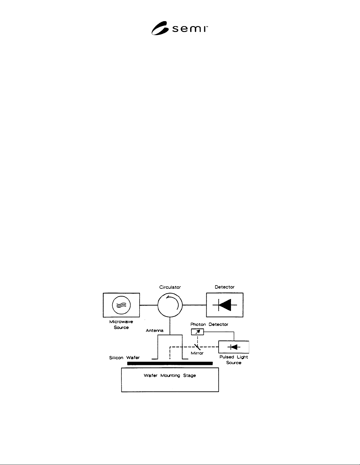
7.2 Photon Detector — Suitable means, such as a
semitransparent mirror in the light path at an angle of
45° and a silicon photodetector, to provide feedback
control to maintain the laser power at a constant level
appropriate to the specified injection level.
7.3 Microwave Pick-Up System — Including a
microwave source operating at a nominal frequency of
10 ± 0.5 GHz and an apparatus for measuring reflected
power, such as a circulator, an antenna, and a detector
(see Figure 1). The sensitivity of the detection system
shall be as great as possible to permit measurement of
photoconductivity decay at low injection levels.
Figure 1
Example Block Diagram of Pulsed Light and Microwave Systems