semi合集-English.pdf - 第7499页
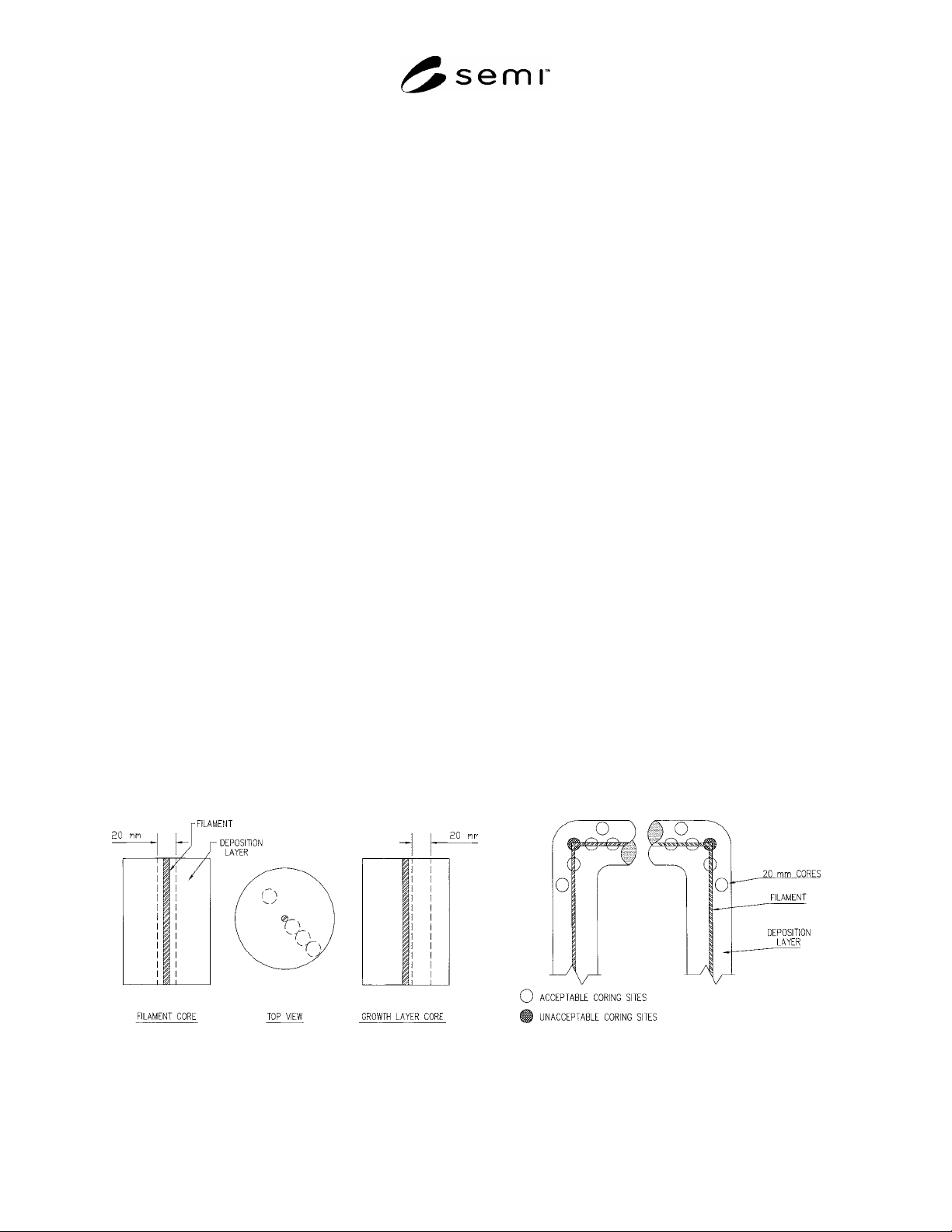
SEMI MF1723-1104 © SEMI 2004 5 10.2.1 Parallel Cores — As shown in Figure 1 , cores are taken paral lel to the filament at a m inimum length of 100 mm and a di ameter of 20 mm. Two different cores, a filament core and a …
SEMI MF1723-1104 © SEMI 2004 4
7.3.2 Scale — Calibrated in mm, suitable for accurate
measurement of ingot length and marking locations in
the ingot for cutting.
7.3.3 Wire Brush — Made of stainless steel, suitable
for cleaning the inside of the chamber of the vacuum
zoner, with a handle long enough to reach the length of
the chamber.
7.3.4 Vacuum Cleaner — Suitable for clean room use,
with flexible hose and narrow nozzle.
7.3.5 Clean Room Gloves — Gowns, Masks, Hoods,
Wipes, and other clean room materials.
7.3.6 Wafering Saw — Suitable for cutting wafer
samples, about 2-mm thick, from the ingot.
8 Reagents
8.1 Nitric Acid (HNO
3
) — In accordance with Grade 2
of SEMI C35.
8.2 Hydrofluoric Acid (HF) — In accordance with
Grade 2 of SEMI C28.
8.3 Acid Etching Mixture — Typically 4 to 1 to 8 to 1
HNO
3
to HF.
8.4 Deionized Water — With a purity equal to or
greater than that specified for Type E-2 in ASTM
D 5127.
8.5 Argon Purge Gas — In accordance with SEMI
C3.42.
9 Hazards
9.1 It is required that the user have a working
knowledge of fabrication techniques, acid handling
practices, and crystal growth furnaces. Good laboratory
practices also must be understood.
9.2 This practice uses hot acid to etch away the surface
of the polysilicon rod. The etchant is potentially
harmful and must be handled in an acid exhaust fume
hood with utmost care at all times. Hydrofluoric acid
solutions are particularly hazardous. All precautions
normally used with these acids should be strictly
observed. They should not be used by anyone who is
not familiar with the specific preventative measures and
first aid treatments given in the appropriate Material
Safety Data Sheet.
9.3 The crystal growth furnace uses radio frequency
(RF) power (generator and coil) to supply power for
melting silicon, about 1400°C. The user must be
trained in working with electrical connections, pressu-
rized gas lines, RF fields, and hot parts.
9.4 The molten silicon in the melt zone emits a bright
light and operators may be exposed to this light for
several hours. This exposure requires the use of eye
protection.
10 Sampling
10.1 The cores shall contain material representative of
the growth process used to form the polysilicon rod.
The cores are intended to be representative of the
polysilicon rod being sampled.
10.2 A number of cores can be taken at different
locations of the polysilicon rod to satisfy various
sample plans. Samples taken should cover both ends of
the rod. Two typical sampling methods are taking cores
parallel to the filament and taking cores perpendicular
to the filament as shown in Figures 1 and 2. The
parallel core system is described in Section 10.2.1. The
perpendicular core system is described in Section
10.2.2.
Figure 1 Figure 2
Parallel Coring Location Perpendicular Coring Locations

SEMI MF1723-1104 © SEMI 2004 5
10.2.1 Parallel Cores — As shown in Figure 1, cores
are taken parallel to the filament at a minimum length
of 100 mm and a diameter of 20 mm. Two different
cores, a filament core and a growth layer core, are
required to calculate the total polysilicon rod impurity
content.
10.2.1.1 Parallel Filament Cores — Cores including
the filament are representative of the filament and the
initial deposition layer on the filament. These cores are
float zoned, analyzed, and the values combined with the
growth layer cores to calculate a total value.
10.2.1.2 Parallel Growth Layer Cores — Cores not
including the filament, only the growth layer, are
representative of the poly deposited onto the filament.
These cores are float-zoned, analyzed, and the values
combined with the filament core values to calculate a
total value.
10.2.1.3 Parallel Core Sampling Locations
10.2.1.3.1 Radial Location — Cores can be taken
across the entire rod diameter to check radial uniformity
of the deposition layer. Since the outer surface may
contain surface cracks or surface roughness, the outer 5
mm should not be sampled.
10.2.1.3.2 Axial Location — For an entire U-rod of
polysilicon, cores usually are taken from the short
bridging section or from a region on the long rod within
50 mm of either end, but may be taken at any location
to check axial uniformity of deposition.
10.2.2 Perpendicular Cores — As shown in Figure 2,
20-mm diameter cores are taken through the diameter
of the polysilicon rod with length same as the diameter
of the poly rod. Cores are taken so that the filament
and material from all parts of the deposition layer are
included. For accurate calculation of the impurities at
various growth layers, at least one end of the perpen-
dicular core should include the outer skin layer. For
rods less than 60-mm diameter, it is not possible to
produce single crystal ingots of sufficient zone length
for accurate analysis. In this case, cores parallel to the
filament are taken for analysis.
10.2.2.1 Perpendicular Growth Layer Cores — Cores
without the intersected filament, as shown in Figure 2,
can be zoned and analyzed to determine the impurities
in the deposition layer. To find the impurities in the
total rod, the filament must be analyzed separately and
combined with the growth layer results. Values are
calculated using the formulas for parallel cores.
10.2.2.2 Perpendicular Core Sampling Location —
For an entire U-rod of polysilicon, cores usually are
taken from the short bridging section, or from a region
on the long rod within 50 mm of either end. Cores may
be taken at any location to check axial uniformity of
deposition, but are not taken at the bend of the U-rod,
due to stresses in this area.
10.3 Filament Analysis — If a parallel or perpendicular
filament core can not be taken, the filament may be
analyzed separately, then combined with the growth
layer analysis. For filaments that are single crystal, or
nearly single crystal, wafers can be cut, prepared, and
analyzed by spectrophotometric techniques described in
SEMI MF1389, SEMI MF1391, and SEMI MF1630.
11 Reference Specimens
11.1 Use polysilicon control rods to monitor the purity
of the core preparation techniques, acid etch bath, and
zoning conditions. Drill a large number of deposition
layer cores, 20-mm diameter by 100-mm length from
polysilicon rods having a uniform deposition layer.
Select control rods with low impurity levels, such as
acceptor/donor values about 0.01 ppba and carbon
values about 0.05 ppma to allow the early detection of
trace impurities from interference sources. After re-
peated analysis, assign values for donor, acceptor, and
carbon concentrations. Then etch, zone, and analyze
these control rods on a periodic basis to monitor purity
of the sample preparation, etching, and zoning pro-
cesses.
11.2 Control chart values for the acceptor, donor, and
carbon concentrations from the control rods using
standard statistical process-control techniques and
statistical rules to determine if the current values are in
control. If these values exceed the statistical limits,
make corrections and repeat the analysis.
12 Procedure
12.1 Seed Preparation
12.1.1 Prepare round or rectangular seeds by core
drilling, cutting, or crystal pulling from high purity float
zone ingots. Use seed material of zero dislocation
density with acceptor content less than 0.05 ppba, donor
content less than 0.05 ppba, and carbon content less
than 0.1 ppma.
12.1.2 Select a high purity single crystal seed, 3 mm to
5 mm in diameter, for initiation of float zone crystal
growth. Orient the seed 111 within 0.5°.
12.1.3 Clean, acid etch, rinse and dry the seed to the
same procedure, using the same equipment described
for core samples. To avoid surface contamination, use
seeds within 36 h after etching, or store them in a
manner to prevent contamination.

SEMI MF1723-1104 © SEMI 2004 6
12.2 Core Etching
12.2.1 Do all operations in the etch bench clean room
and zoner clean room with operators in full clean room
attire, including gloves, hood, and mask.
12.2.2 Make a fresh acid etch mixture and fill the tanks
in the etch bench. When the proper temperatures and
water flows are achieved, place the core samples into
clean etch boats and etch, rinse, and dry the cores. Use
the HNO
3
-HF acid etching mixture, etching at least two
cycles, to remove a minimum of 100 m from the
surface of the core sample. This is necessary in order to
remove surface damage caused by the coring process.
Other acid etch mixtures can be used, but must be
evaluated and controlled to ensure effectiveness and
avoid impurity interferences.
12.2.3 After etching, float zone cores as soon as
possible to reduce the probability of contamination.
Re-etch cores if the maximum holding period is
exceeded. To extend the holding period, seal the cores
in a suitably clean material and store in a clean room
environment.
12.3 Preparation of Apparatus
12.3.1 Clean the core drilling apparatus to prevent
contamination of the core sample.
12.3.2 Clean the etch bench and check the DI rinse
water purity, temperature, total organic carbon, and
resistivity.
12.3.3 Clean the float zone chamber. Using the stain-
less steel wire brush, scrub the walls of the chamber to
loosen silicon deposits and remove the loose particles
with the vacuum cleaner. Wipe the walls, holders, and
coil with clean room wipes soaked with a high purity
solvent. Inspect cooling water reservoir, water flow,
water temperature, coil and preheater connections,
shaft, coil feedthroughs, door seals, hose connections,
travel stops, and rotations.
12.3.4 Carry out major cleaning, including acid
cleaning of coil and associated parts, and changing of
seals on a periodic basis. After cleaning, argon drying,
and vacuum pumping, perform a chamber and preheater
bakeout of at least 15 min.
12.4 Ingot Growth
12.4.1 Place the core samples and seed in the furnace
chamber so that both hang plumb and are centered and
aligned with the vertical axis of rotation.
12.4.2 Remove air from the chamber with a series of
evacuation and argon purge cycles. Fill the chamber
with argon and continue the argon purge throughout the
growth cycle, maintaining a positive pressure of argon
in the chamber.
12.4.3 Position the seed end of the core sample in the
coil, and the preheater close to the seed end of the core.
Adjust the preheater power to make the initial induction
coupling of the preheater and sample, and heat until the
sample begins to glow, about 600 to 700°C. Move the
preheater away from the sample and move the core
sample close to the coil opening to establish a molten
zone controlled by power to the coil.
12.4.4 After a small molten zone has been established
at the seed end, move the seed vertically until it touches
the molten zone. Withdraw the seed to form a conical
melt, making sure the seed has melted in, and begin the
necking phase in order to form a zero dislocation
crystal.
12.4.5 Adjust top and bottom travel and rotation rates
to complete the necking phase, check for the three-
growth facet lines to ensure the ingot is single crystal,
and adjust travel and power level to form the final
diameter of the ingot. Adjust the travel and rotations
and grow a single crystal zero dislocation ingot.
12.4.6 When the desired ingot length has been attained,
pull the ingot from the melt, making sure the ingot and
melt separate without freezing. After separation,
reduce power, stop all travels and rotation, turn off
power, and allow to cool.
12.5 Ingot Evaluation
12.5.1 Visual Examination — Examine the ingot
visually for uniformity of diameter, continuous
uniform-growth facet line, and color, to determine
whether the ingot is zero dislocation single crystal and
whether oxide deposits are present as a result of air
leaks.
12.5.2 Structural and Electrical Examination
12.5.2.1 Determine crystallographic orientation in ac-
cordance with SEMI MF26 on a sampling basis to
confirm the visual examination.
12.5.2.2 Determine the crystallographic perfection of
the grown ingot in accordance with SEMI MF1725 on a
sampling basis to confirm the visual examination.
12.5.2.3 Test for uniform distribution of
acceptor/donor impurities by plotting a resistivity
profile along the length of the ingot in accordance with
SEMI MF397. Note that resistivity values should vary
along the length consistent with the net acceptor/donor
values measured at the various points and that sharp
changes in the profile indicate point contamination or
nonuniformity of the sample deposition layer.
12.6 Ingot Sampling
12.6.1 After the ingot is inspected for crystallographic
perfection, appearance, and uniformity, and judged to