semi合集-English.pdf - 第7550页
SEMI MF1810-0304 © SEMI 2003, 2004 3 Figure 2 Four Scan, Multiple Micros copic Inspection Patter n 9.2 Defect Density Calculation 9.2.1 Count each defect class separately for each diameter scanned. Calculat e the total a…
SEMI MF1810-0304 © SEMI 2003, 2004 2
NOTICE: Unless otherwise indicated, all documents
cited shall be the latest published versions.
5 Terminology
5.1 Definitions of terms related to silicon technology
are found in SEMI M1 and SEMI MF1241.
6 Summary of Test Method
6.1 Samples for this test are selected and prepared in
accordance with SEMI MF1725, SEMI MF1726 or
SEMI MF1727. As indicated in these practices, the
defect to be analyzed is exposed using one of the
specific etching solutions listed in SEMI MF1809.
6.2 The wafer is aligned on a microscope stage.
6.3 It is then inspected according to predefined
inspection pattern.
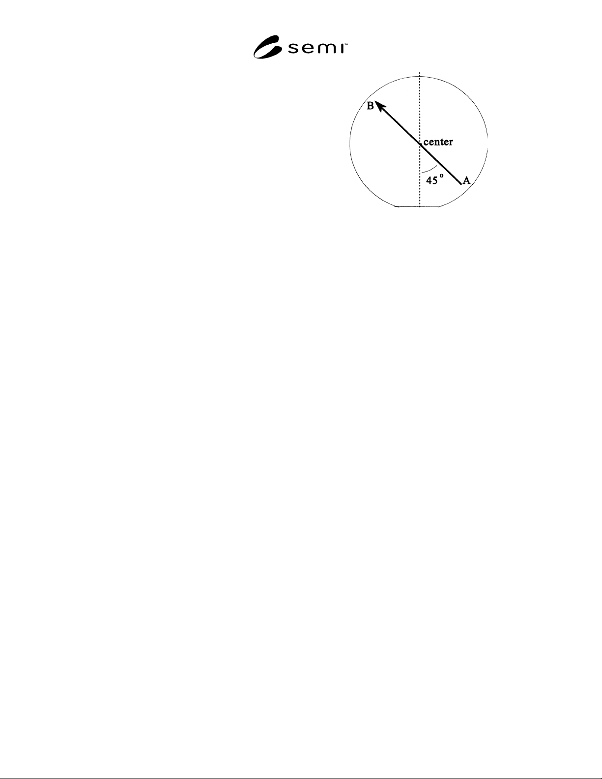
6.3.1 The basic inspection pattern is a single scan along
a wafer diameter. The starting and ending points of the
scan pattern are 5 mm from the edges of the wafer.
Figure 1 represents the characteristics of the basic
pattern.
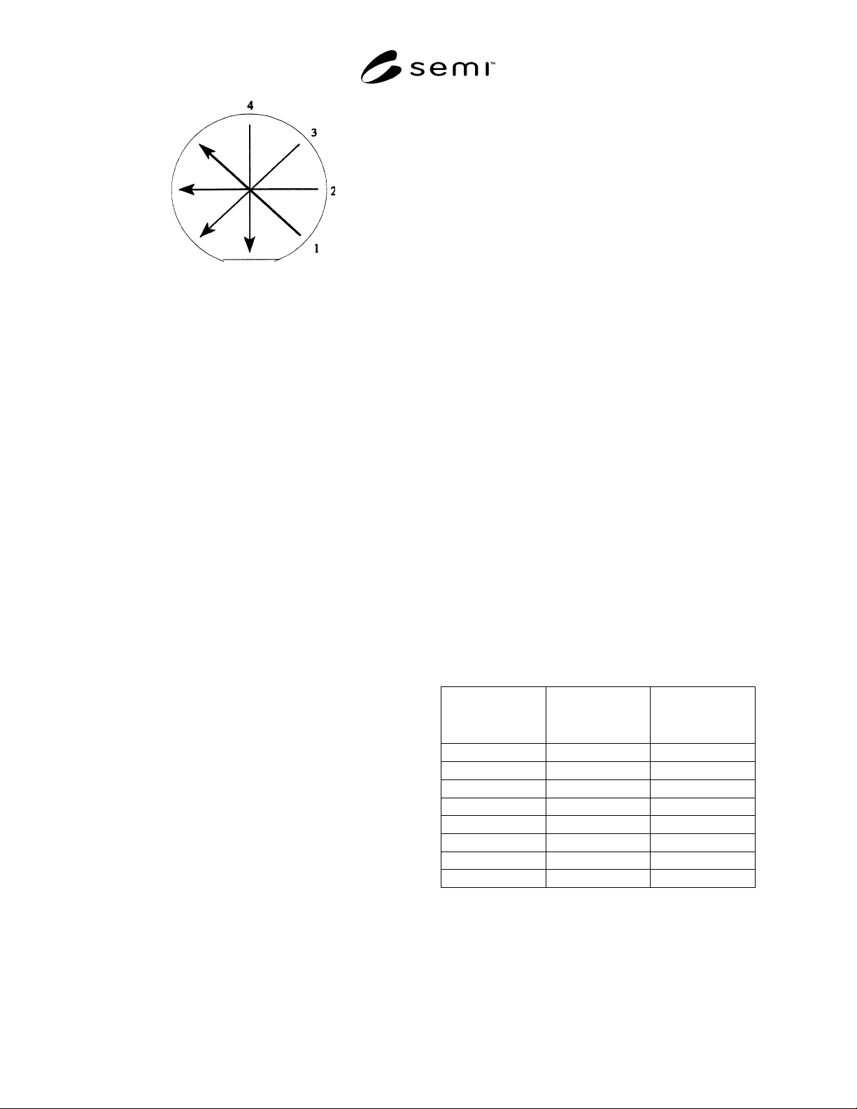
6.3.2 The complete inspection pattern of this test
method is based upon the combination of four separate
basic scans across different diameters.
6.4 Finally, specific defects distinguished by shape or
size are counted.
7 Apparatus
7.1 Nonmetallic Vacuum Pickup Tool — Of suitable
material such as quartz or TFE-fluorocarbon. The
pickup tool shall be constructed so that no metal can
contact the specimen wafer.
7.2 Optical Microscope — Equipped with interference
contrast attachment.
NOTE 3: Nomarski differential interference contrast is an
example of interference contrast.
7.2.1 Eyepiece and Objective Lens — In combination
shall give a magnification range of approximately 100×
to 400× magnification of the specimen. The dimension
of the field of view at each magnification option is
calibrated to allow defect density calculations.
NOTE: Begin scan 5 mm from the edge.
Figure 1
The Basic Microscopic Inspection Scan Pattern
7.2.2 Graduated Metric X-Y Microscope Stage — Used
for sample positioning.
8 Sampling
8.1 Specimens shall be selected to represent the lot to
be tested as specified in producer-consumer
agreements.
9 Procedure
9.1 Four Scan Inspection Pattern
9.1.1 Place the specimen wafer onto the microscope
inspection stage. Handle wafers only with a clean
nonmetallic vacuum pickup tool to avoid scratching or
contaminating the surface.
9.1.2 Place the specimen such that a single linear
motion of the stage (either x or y) allows counting of
defects contained in the field of view along the path
labeled AB in Figure 1. Points A and B are 5 mm from
the wafer edge and the line AB is rotated 45° from the
location of the major orientation flat or notch.
Alternative edge exclusion positions are acceptable
with the agreement of the parties involved.
9.1.3 Scan the path and record the classification and
numbers of the defects observed during the scan. Refer
to descriptions and pictures in SEMI MF1809.
9.1.4 Rotate the wafer by 45° clockwise on the
microscope stage and repeat Section 9.1.3 for the
second scan. Refer to Figure 2 for improved definition
of the scan pattern.
9.1.5 Rotate the wafer by 45° clockwise on the
microscope stage and repeat Section 9.1.3 for the third
scan.
9.1.6 Rotate the wafer by 45° clockwise on the
microscope stage and repeat Section 9.1.3 for the fourth
scan.
SEMI MF1810-0304 © SEMI 2003, 2004 3
Figure 2
Four Scan, Multiple Microscopic Inspection Pattern
9.2 Defect Density Calculation
9.2.1 Count each defect class separately for each
diameter scanned. Calculate the total area inspected by
multiplying four (4) times the calibrated width of the
field of view in centimeters by the length of the scan in
centimeters. The length (L) in centimeters is the wafer
diameter (D) in centimeters minus twice the 0.5 cm
edge exclusion (E):
0.12 −=−= DEDL (1)
The density is the defect count divided by the total area.
NOTE 4: When a scan intersects a flat, notch or laser mark,
the total area must be adjusted according to the reduced length
of the affected scans. Failure to adjust the area results in
inaccuracy.
10 Report
10.1 Report the following information:
10.1.1 Date of test, laboratory and operator,
10.1.2 Identification of the specimen wafer,
conductivity type, orientation, and diameter,
10.1.3 Specimen history; thermal cycle, preferential
etchant formulation, thickness removal during
preferential etching,
10.1.4 Inspection conditions; magnification, and total
area inspected, and
10.1.5 Defect density and precision by defect
classification.
11 Precision and Bias
11.1 Precision — The multi laboratory precision of
this test method was established through a round-robin
experiment. Seven (7) wafers with randomly
distributed oxidation induced stacking faults (OISFs)
were analyzed by sixteen (16) laboratories over eleven
(11) diameter scans. Repeatability and reproducibility
of this test method were calculated using two sets of
four scan measurements from each laboratory and
wafer. The wafer samples were prepared according to
SEMI MF1727 and etched with Wright Etch in
accordance with SEMI MF1809.
11.1.1 Repeatability — The method repeatability is
equal to 2.8 times the within-laboratory standard
deviation or 5.22 defects/cm
2
. Repeatability contributes
23.81% of the total variation. The variability of the
measurement is sample dependent; assumptions of
random OISF location were described as a limitation
(see Section 3.3).
11.1.2 Reproducibility — The method reproducibility
is equal to 2.8 times the between-laboratory standard
deviation or 9.31 defects/cm
2
. Reproducibility
contributes 75.73% of the total variation.
NOTE 5: Additional analysis is presented in Related
Information 1. A study of two repetitions of this test method
was extracted from the existing, multiple scan data measured
at each laboratory.
11.1.3 The wafers exhibited single diameter scans that
ranged from 0 to 13 defects/cm
2
while the grand
average of all measurements for each wafer yielded
densities of 0.21 to 3.60 defects/cm
2
. The range in
measurement density is related to differences between
laboratories and local variation of the defect density on
the wafer itself.
11.1.4 Ten separate diameters were measured on each
of 7 wafers by 16 laboratories. The total number of
scans for each sample was 160. Table 1 shows the
sample dependence of the results with the standard
deviation versus mean OISF count for ten independent
scans.
Table 1 Ten Scan Inspection Data
Wafer Identity
Standard
Deviation
Mean OISF
Density All Data
(OISF/cm
2
)
A 0.49 0.21
B 1.79 1.43
C 1.93 1.98
D 1.02 0.82
E 2.51 3.60
F 0.63 0.42
G 0.71 0.51
ALL 1.49 1.28
11.2 Bias — No standard reference materials are
available to calibrate this measurement; therefore a
target density for each wafer was assigned by averaging
the combined data from all scans of each wafer.
Analysis of the round robin is based upon the individual
deviation from the target for each measurement and

SEMI MF1810-0304 © SEMI 2003, 2004 4
sample. The method bias is estimated using the average
range of the location deviations from the target for the
round-robin results or 2.11 defects/cm
2
.
12 Keywords
12.1 defect density; dislocation; grain boundary;
microscopic; polycrystalline imperfection; preferential
etch; silicon; slip