semi合集-English.pdf - 第7582页
SEMI MF2139-1103 © SEMI 2003 2 charged particle activation analysis d etection capability is limit ed by an int erference from boron. NOTICE : This standard does not purpor t to address the safety issues, if any, associa…

SEMI MF2139-1103 © SEMI 2003 1
SEMI MF2139-1103
TEST METHOD FOR MEASURING NITROGEN CONCENTRATION IN
SILICON SUBSTRATES BY SECONDARY ION MASS SPECTROMETRY
This standard was technically approved by the Global Silicon Wafer Committee and is the direct
responsibility of the North American Silicon Wafer Committee. Current edition approved for publication by
the North American Regional Standards Committee on July 27, 2003. Initially available at www.semi.org
October 2003; to be published November 2003. Originally published by ASTM International as ASTM
F 2139-01. Last previous edition ASTM F 2139-01.
1 Purpose
1.1 Secondary ion mass spectrometry (SIMS) can
measure in un-annealed, polished Czochralski (CZ)
silicon substrates the nitrogen concentration that may
be intentionally introduced to: (1) increase the V/G
tolerance for grown-in defects free region, where V is
the pull rate and G is the crystal temperature gradient at
the solid-liquid interface;
1
(2) increase the void-free
denuded zone depth and the bulk micro-defect density
after annealing in hydrogen or argon;
2,3
(3) reduce the
crystal originated particle (COP) size after annealing;
2,3
or (4) enhance the precipitation of oxygen in epitaxial
substrates under reduced temperature processing.
4
1.2 SIMS can measure total bulk nitrogen in CZ-
silicon, whereas infrared spectroscopy is negatively
affected by the chemical state in oxygen-containing
silicon.
5
In addition, SIMS can measure the total bulk
nitrogen in p
+
(B) and n
+
(Sb) substrates used for
epitaxial silicon, whereas infrared spectroscopy cannot
due to free electron absorption interferences.
1.3 SIMS can measure in un-annealed, polished Float-
zoned (FZ) silicon substrates the nitrogen concentration
1 Iida, M., Kusaki, W., Tamatsuka, M., Iino, E., Kimura, M., and
Muraoka, S., “Effects of Light Element Impurities on the Formation
Grown-In Defects Free Region of Czochralski Silicon Single
Crystal,” in Defects in Silicon III, edited by W. M. Bullis, W. Lin, P.
Wagner, T.Abe, and S. Kobayashi, The Electrochemical Society
Proceedings Series PV99-1 (The Electrochemical Society,
Pennington, NJ, 1999) pp. 499-510.
2 Tamatsuka, M., Kobayashi, N., Tobe, S., and Masui, T., “High
Performance Silicon Wafer with Wide Grown-in Void Free Zone and
High Density Internal Gettering Site Achieved via Rapid Crystal
Growth with Nitrogen Doping and High Temperature Hydrogen
and/or Argon Annealing,” ibid., pp.456-467.
3 Minami, T., Takeda, R., Saito, H., Hirano, Y., Suzuki, O., Nitta, S.
Kashima, K., and Matsushita, Y., “Influence of Void Size on the
Formation of Defect Free Regions in Hydrogen Annealed CZ Silicon
Wafers,” ECS Extended Abstract No.514, 197th Meeting of the
Electrochemical Society, (The Electrochemical Society, Pennington,
NJ, 2000).
4 Shimura, F., and Hockett, R. S., “Nitrogen effect on oxygen
precipitation in Czochralski silicon,” Appl. Phys. Lett. 48, 224-226
(1986).
5 Abe, T., Kikuchi, K., Shirai, S., and Muraoka, M., in Semicon-
ductor Silicon 1981, edited by H. R. Huff, R. J. Kriegler and Y.
Takeishi, (The Electrochemical Society, Pennington, NJ, 1981) pp.
54-71.
that may be introduced to strengthen low oxygen
substrates.
1.4 The SIMS method can be used for process check of
crystal doping, and for research and development.
2 Scope
2.1 This test method covers the determination of total
nitrogen concentration in the bulk of single crystal
substrates using secondary ion mass spectrometry
(SIMS).
6,7
2.2 This test method can be used for silicon in which
the dopant concentrations are less than 0.2% (1 × 10
20
atoms/cm
3
) for boron, antimony, arsenic, and
phosphorus.
2.3 This test method is for bulk analysis where the
nitrogen concentration is constant with depth.
2.4 This test method can be used for silicon in which
the nitrogen content is 1 × 10
14
atoms/cm
3
or greater.
The detection capability depends upon the SIMS
instrumental nitrogen background and the precision of
the measurement.
2.5 This test method is complementary to infrared
spectroscopy, electron paramagnetic resonance, deep
level transient spectroscopy, and charged particle
activation analysis.
8
The infrared spectroscopy method
detects nitrogen in specific vibrational states, rather
than total nitrogen, and is limited to silicon with doping
concentrations less than about 1 × 10
17
atoms/cm
3
. The
6 Hockett, R. S., Evans, Jr., C. A., and Chu, P. K., “The SIMS
Measurement of Nitrogen in Nitrogen-Doped CZ-Silicon,” in
Secondary Ion Mass Spectrometry SIMS VI, edited by A.
Benninghoven, A. M. Huber, and H. W. Huber, (John Wiley & Sons,
New York, 1988) pp. 441-444.
7 Hockett, R. S. and Sams, D. B., “The Measurement of Nitrogen in
Silicon Substrates by SIMS,” in High Purity Silicon VI, edited by C.
L. Claeys, P. Rai-Choudhury, M. Watanabe, P. Stallhofer, and H. J.
Dawson, ECS Proceedings Vol PV 2000-17 (The Electrochemical
Society, Pennington, NJ, 2000) pp. 584-595.
8 Stein, Herman J., “Nitrogen in Crystalline Si,” in Materials
Research Society Symposia Proceedings Vol 59, Oxygen, Carbon,
Hydrogen and Nitrogen in Crystalline Silicon, edited by J. C.
Mikkelsen, Jr., S. J. Pearton, J. W. Corbett, and S. J. Pennycook,
(Materials Research Society, Pittsburgh, PA, 1986) pp. 523-535.

SEMI MF2139-1103 © SEMI 2003 2
charged particle activation analysis detection capability
is limited by an interference from boron.
NOTICE: This standard does not purport to address the
safety issues, if any, associated with its use. It is the
responsibility of the user of this standard to establish
appropriate safety and health practices and determine
the applicability of regulatory or other limitations prior
to use.
3 Limitations
3.1 Nitrogen on or in the surface silicon oxide can
interfere with the bulk nitrogen measurement.
3.2 Nitrogen adsorbed on the test specimen surface
from the SIMS instrument chamber and fixtures
interfere with the bulk nitrogen measurement by raising
the background signal. The vacuum quality of the
SIMS instrument can be used to minimize this.
3.3 Nitrogen in the SIMS primary Cs beam may be
implanted into the silicon specimen as CsN and thereby
increase the nitrogen background concentration. A
primary beam mass filter may be used to reduce this
interference, but in this case, a reduced Cs beam current
density is needed to maximize the sputter rate.
3.4 Anomalous nitrogen intensity spikes can interfere
with the averaging of signal intensity which is assumed
to be random (see Section 6.9).
3.5 Carbon introduces an interference as
12
C
30
Si at
mass 42 for detecting nitrogen as
14
N
28
Si. This can be
avoided by detecting the nitrogen as
14
N
29
Si at mass 43,
but the signal rate is reduced greatly, about a factor of
20 when the minor isotope of silicon is used. There are
methods to measure the carbon interference, and
subtract this interference. One of the methods to
measure the carbon interference can have its own
interference from high levels of boron dopant.
3.6 The specimen surface must be flat in the specimen
holder window so that the inclination of the specimen
surface with respect to the ion collection optics is
constant from specimen to specimen. Otherwise, the
accuracy and precision can be degraded.
3.7 The bias and precision of the measurement
significantly degrade as the roughness of the specimen
surface increases. This degradation can be avoided by
using chemical-mechanical polished wafers.
3.8 Variability of nitrogen in the calibration specimen
can limit the measurement precision.
3.9 Variability from the calibration measurement may
increase the measurement precision of the test
specimen.
3.10 Bias in the assigned nitrogen concentration of the
calibration specimen can introduce bias into the SIMS
measured nitrogen.
3.11 Thermal processing above 800° C of the silicon
substrate may cause diffusion of the nitrogen, so that
the nitrogen concentration is not constant with depth, a
key assumption of this test method.
3.12 Thermal processing of the silicon substrates in a
nitrogen-containing ambient can introduce large
amounts of nitrogen from the ambient deep into the
silicon crystal.
6
4 Referenced Standards
4.1 ASTM Standards
9
E 122 — Practice for Calculating Sample Size to Esti-
mate, with a Specified Tolerable Error, the Average for
a Characteristic of a Lot or Process
E 673 — Terminology Relating to Surface Analysis
NOTICE: Unless otherwise indicated, all documents
cited shall be the latest published versions.
5 Terminology
5.1 Definitions — all terms in this test method are in
accordance with those given in ASTM Terminology
E 673.
6 Summary of Test Method
6.1 SIMS is utilized to determine the bulk
concentration of nitrogen in single crystal silicon
substrate. Specimens of single crystal silicon (one
calibration specimen and the test specimens) are loaded
into a sample holder. The holder with the specimens is
baked at 100° C in air for 1 h and then transferred into
the analysis chamber of the SIMS instrument.
6.2 The calibration sample is analyzed using a cesium
(Cs) primary ion beam and negative ion spectrometry of
14
N
28
Si, or
15
N
28
Si, depending upon the nitrogen isotope
in the calibration sample, to determine a relative
sensitivity factor (RSF) of nitrogen in silicon.
6.3 Each test specimen in the sample holder is
sputtered by the primary cesium ion beam, without
analyzing secondary ion intensities, in order to reduce
the nitrogen background. The amount of time required
for this pre-analysis sputtering depends upon the
instrumentation and the desired background nitrogen
concentration.
9 Available from ASTM International, 100 Barr Harbor Drive, West
Conshohoken, PA 19428-2959, USA. Telephone: 610.832.9585,
Fax: 610.832-9555, Web site:
www.astm.org. ASTM E 122 is
published in Volume 14.02 of Annual Book of ASTM Standards while
ASTM E 673 is published in Volume 3.06.
SEMI MF2139-1103 © SEMI 2003 3
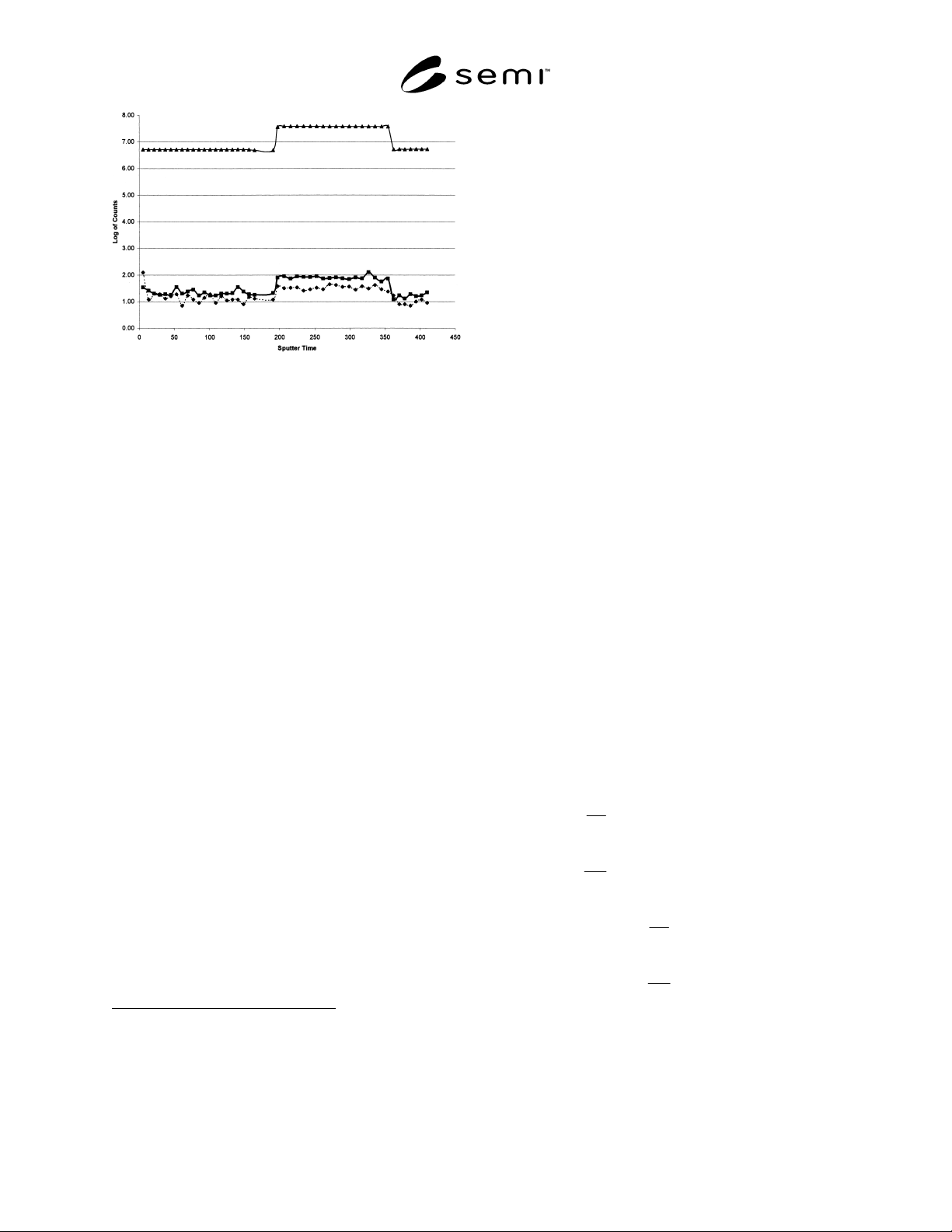
NOTE: Top curve (
!) Mass 30 (
30
Si); middle curve (!)
Mass 42 (
14
N
28
Si), bottom curve (
") Mass 40 (
12
C
28
Si)
Figure 1
SIMS Signals in Nitrogen-Doped Silicon, Log Scale
6.4 For the analysis of the test specimens, a cesium
primary ion beam is used to bombard each test
specimen at two different sputter rates, by reducing the
beam raster area for the second sputter rate, while at the
same time maintaining a constant detected area. This
beam raster change technique is used for two reasons.
Firstly, this technique reduces the background nitrogen
contribution from the sample surface. Secondly, this
technique allows the determination of both the
instrumental nitrogen background and the real bulk
nitrogen concentration in each test specimen
measurement without the use of a separate blank
specimen, and due to averaging is capable of separating
the bulk nitrogen from the instrumental nitrogen even if
the bulk nitrogen is less than the instrumental
nitrogen.
10
6.5 The two sputter rates, and the amount of time they
are applied in each measurement, are chosen to
optimize the detection capability; the values depend on
the instrumentation being used. However, the second
sputter rate is typically the maximum sputter rate of the
instrumentation, and the first sputter rate is typically
less than half that of the second sputter rate.
6.6 The negative secondary ion of
14
N
28
Si is mass
analyzed by a mass spectrometer, and detected by an
electron multiplier (EM) or equivalent high-sensitivity
ion detector as a function of time. The matrix negative
secondary ion count for silicon (
28
Si,
29
Si,
30
Si, or a
10 Ishitani, A., Okuno, K., Karen, A., Karen, S. and Soeda, F.,
“Improvement of Oxygen Detection Limit in Silicon by Use of the
Secondary Ion Energy Distribution and Background Subtraction,” in
Proceedings of the International Conference of Materials and
Process Characterization for VLSI, 1988 (ICMPC'88), edited by X-F
Zong, Y-Y Wang, and J. Chen, (World Scientific, New Jersey, 1988)
pp. 124-129.
dimer such as
30
Si
2
) is measured by a Faraday cup (FC)
or appropriate detector during the profile. If multiple
detectors are used during the test, the relative
sensitivities of the detectors are determined by
measuring standard ion signals (either the same
negative secondary ion count rate or ion count rates of
known relative intensity such as natural
28
Si/
30
Si) on
each detector. Additional negative secondary ions of
11
B
28
Si,
12
C, and
12
C
28
Si may also be detected depen-
ding upon the boron and carbon concentration in the
test specimen.
6.7 For illustration purposes an example data profile is
shown in Figure 1 where the log of counts of
12
C
28
Si,
14
N,
28
Si, and
30
Si is plotted versus sputter time. At
about 200 s, the Cs beam raster area was changed from
250 µm × 250 µm down to 50 µm × 50 µm, resulting in
an increase in signal intensities, because the volume of
material analyzed per second has increased. At about
350 s, the Cs beam raster area was reversed back to the
first condition, and the signal intensities are seen to be
reduced back to the original levels. Since the surface
analysis area was kept constant during the raster change
(that is, the actual surface area detected is independent
of the raster area), the signal intensities have two
separate contributions, one from elements that are
adsorbed to the surface and one from elements in the
volume of material analyzed each second. There is
some nitrogen (and carbon in this case) that is adsorbed
to the surface from the local environment outside of the
silicon, and there is some nitrogen that is from the bulk
silicon. A key point is that if there is no nitrogen in the
bulk silicon, the nitrogen signal intensity does not
change as a result of the change in sputter rate, because
the adsorbed nitrogen (that is, instrumental nitrogen
signal) is only dependent on the analysis area, which
has been held constant. This understanding leads to the
following equations:
][][ NNRSF
I
I
b
si
n
+=× (1)
][][ NNRSF
I
I
B
SI
N
+=× (2)
RSF
I
I
N
si
B
b
×=][ (3)
RSF
I
I
N
SI
B
B
×=][ (4)
where:
I
n
= secondary ion intensity of
14
N
28
Si under the
higher sputter rate conditions,
I
N
= secondary ion intensity of
14
N
28
Si under the
lower sputter rate conditions,