semi合集-English.pdf - 第7584页
SEMI MF2139-1103 © SEMI 2003 4 [ N b ] = contribution of backgro und nitroge n to the observed nitroge n concent ration under the higher sputter rate conditions, [ N B ] = contribut ion of backgr ound nitrogen to the obs…
SEMI MF2139-1103 © SEMI 2003 3
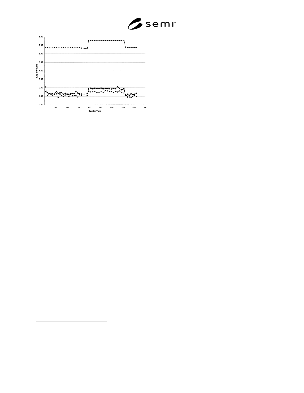
NOTE: Top curve (
!) Mass 30 (
30
Si); middle curve (!)
Mass 42 (
14
N
28
Si), bottom curve (
") Mass 40 (
12
C
28
Si)
Figure 1
SIMS Signals in Nitrogen-Doped Silicon, Log Scale
6.4 For the analysis of the test specimens, a cesium
primary ion beam is used to bombard each test
specimen at two different sputter rates, by reducing the
beam raster area for the second sputter rate, while at the
same time maintaining a constant detected area. This
beam raster change technique is used for two reasons.
Firstly, this technique reduces the background nitrogen
contribution from the sample surface. Secondly, this
technique allows the determination of both the
instrumental nitrogen background and the real bulk
nitrogen concentration in each test specimen
measurement without the use of a separate blank
specimen, and due to averaging is capable of separating
the bulk nitrogen from the instrumental nitrogen even if
the bulk nitrogen is less than the instrumental
nitrogen.
10
6.5 The two sputter rates, and the amount of time they
are applied in each measurement, are chosen to
optimize the detection capability; the values depend on
the instrumentation being used. However, the second
sputter rate is typically the maximum sputter rate of the
instrumentation, and the first sputter rate is typically
less than half that of the second sputter rate.
6.6 The negative secondary ion of
14
N
28
Si is mass
analyzed by a mass spectrometer, and detected by an
electron multiplier (EM) or equivalent high-sensitivity
ion detector as a function of time. The matrix negative
secondary ion count for silicon (
28
Si,
29
Si,
30
Si, or a
10 Ishitani, A., Okuno, K., Karen, A., Karen, S. and Soeda, F.,
“Improvement of Oxygen Detection Limit in Silicon by Use of the
Secondary Ion Energy Distribution and Background Subtraction,” in
Proceedings of the International Conference of Materials and
Process Characterization for VLSI, 1988 (ICMPC'88), edited by X-F
Zong, Y-Y Wang, and J. Chen, (World Scientific, New Jersey, 1988)
pp. 124-129.
dimer such as
30
Si
2
) is measured by a Faraday cup (FC)
or appropriate detector during the profile. If multiple
detectors are used during the test, the relative
sensitivities of the detectors are determined by
measuring standard ion signals (either the same
negative secondary ion count rate or ion count rates of
known relative intensity such as natural
28
Si/
30
Si) on
each detector. Additional negative secondary ions of
11
B
28
Si,
12
C, and
12
C
28
Si may also be detected depen-
ding upon the boron and carbon concentration in the
test specimen.
6.7 For illustration purposes an example data profile is
shown in Figure 1 where the log of counts of
12
C
28
Si,
14
N,
28
Si, and
30
Si is plotted versus sputter time. At
about 200 s, the Cs beam raster area was changed from
250 µm × 250 µm down to 50 µm × 50 µm, resulting in
an increase in signal intensities, because the volume of
material analyzed per second has increased. At about
350 s, the Cs beam raster area was reversed back to the
first condition, and the signal intensities are seen to be
reduced back to the original levels. Since the surface
analysis area was kept constant during the raster change
(that is, the actual surface area detected is independent
of the raster area), the signal intensities have two
separate contributions, one from elements that are
adsorbed to the surface and one from elements in the
volume of material analyzed each second. There is
some nitrogen (and carbon in this case) that is adsorbed
to the surface from the local environment outside of the
silicon, and there is some nitrogen that is from the bulk
silicon. A key point is that if there is no nitrogen in the
bulk silicon, the nitrogen signal intensity does not
change as a result of the change in sputter rate, because
the adsorbed nitrogen (that is, instrumental nitrogen
signal) is only dependent on the analysis area, which
has been held constant. This understanding leads to the
following equations:
][][ NNRSF
I
I
b
si
n
+=× (1)
][][ NNRSF
I
I
B
SI
N
+=× (2)
RSF
I
I
N
si
B
b
×=][ (3)
RSF
I
I
N
SI
B
B
×=][ (4)
where:
I
n
= secondary ion intensity of
14
N
28
Si under the
higher sputter rate conditions,
I
N
= secondary ion intensity of
14
N
28
Si under the
lower sputter rate conditions,
SEMI MF2139-1103 © SEMI 2003 4
[N
b
] = contribution of background nitrogen to the
observed nitrogen concentration under the
higher sputter rate conditions,
[N
B
] = contribution of background nitrogen to the
observed nitrogen concentration under the
lower sputter rate conditions,
I
B
= secondary ion intensity from the adsorbe
d
b
ackground nitrogen under both sputter rate
conditions,
I
si
= secondary ion intensity of the silicon matrix
(e.g.,
30
Si) under the higher sputter rate
conditions,
I
SI
= secondary ion intensity of the silicon matrix
(e.g.,
30
Si) under the lower sputter rate
conditions,
RSF = relative sensitivity factor for converting the ion
intensity ratio to concentration, and
[N] =
b
ulk nitrogen concentration in the test
specimen.
6.8 Equations (1) through (4) can be used to determine
[N] and [N
b
] from measured data as follows:
)/(1
)/(1
][
siSI
nN
si
n
II
II
I
I
RSFN
−
−
××= (5)
][][ N
I
I
RSFN
si
n
b
−×= (6)
In these equations, the secondary ion intensities used
are averages of these signal intensities. In the example
shown in Figure 1, the lower sputter rate was used at
the beginning of the profile, and the higher sputter rate
in the middle of the profile. For this example, [N] was
determined to be 8 × 10
14
/cm
3
and [N
b
] was 2 ×
10
14
/cm
3
. The use of averages for I
n
and I
N
is
particularly critical for detecting low levels of nitrogen
where the signal intensity count rates can be low and
therefore noisy. By using averages, it is possible to
detect an [N] level that is less than [N
b
] in the analysis.
6.9 The SIMS measurement of nitrogen in bulk-doped
silicon sometimes reveals anomalous intensity spikes
that are greater than a random fluctuation of signal
intensity, even in silicon that has not been thermally
processed beyond crystal growth.
6,7
These nitrogen
intensity spikes are not well understood, but are
suspected to be associated with oxygen defects,
possibly a co-aggregation of nitrogen and oxygen in a
precipitate form. Similar SIMS effects have been well
known for oxygen and even carbon in thermally-
processed silicon.
11
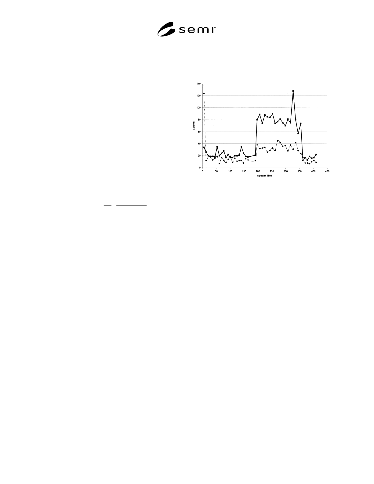
Figure 2 shows an expanded view
of the carbon and nitrogen data taken from Figure 1.
11 Hockett, R. S., Fraundorf, P. B., Reed, D. A., and Wayne, D. R.,
“Oxygen and Carbon Defect Characterization in Silicon by SIMS,” in
Oxygen, Carbon, Hydrogen and Nitrogen in Crystalline Silicon,
edited by J. C. Mikkelsen, Jr., S. J. Pearton, J. W. Corbett, and S. J.
Pennycook, Materials Research Society Symposia Proceedings Vol
59 (Materials Research Society, Pittsburgh, PA, 1986) pp. 433-438.
The vertical scale is linear. The unusually high
nitrogen signal at about 325 s may be one of these
anomalous intensity spikes. The presence of such non-
random signals, if significant, can make the averaging
method used here questionable.
NOTE: Top curve (
!) Mass 42 (
14
N
28
Si), bottom curve
(
") Mass 40 (
12
C
28
Si)
Figure 2
SIMS Signals from Nitrogen-Doped Silicon, Linear
Scale
6.10 Depending upon the carbon concentration in the
test specimen and the level of nitrogen, it may be
necessary to correct the
14
N
28
Si signal for an interfer-
ence from
12
C
30
Si. This correction is done by co-
detecting
12
C
28
Si at mass 40, and calculating the
contribution of
12
C
30
Si from isotopic ratios. The
contribution to mass 42 from a carbon-related signal at
mass 40 is 0.0341 times the signal at mass 40. In the
example in Figure 1, where the actual carbon concen-
tration is about 1.5 × 10
15
/cm
3
by SIMS calibration, the
carbon interference is insignificant. A carbon concen-
tration of 5 × 10
15
/cm
3
(the detection limit of most
Fourier Transform Infrared (FITR) measurements of
carbon in silicon) corresponds to an interference equi-
valent to about 8 × 10
13
/cm
3
of nitrogen. Thus, in
detecting nitrogen in the low 10
14
/cm
3
level, a co-
measurement of the carbon interference is critical.
6.11 Depending upon the boron concentration in the
test specimen, the procedure to correct for the carbon
interference may need to be modified by detecting
11
B
28
Si at mass 39, and calculating the contribution of
11
B
29
Si and
10
B
30
Si at mass 40. This procedure
becomes important for test specimens with boron
concentrations at 1 × 10
17
/cm
3
and greater. In the
example in Figure 1, the boron concentration is on the
order of 10
15
/cm
3
and does not interfere.

SEMI MF2139-1103 © SEMI 2003 5
7 Apparatus
7.1 SIMS Instrument — Equipped with a cesium
primary ion source, electron multiplier detector, and
Faraday cup detector, capable of measuring negative
secondary ions. The SIMS instrument should be
adequately prepared (that is, baked) so as to provide the
lowest possible instrumental background, since the
instrumental background can affect the detection
capability. High quality vacuum is desired. A liquid
nitrogen- or liquid helium-cooled cryopanel, which
surrounds the test specimen holder in the analysis
chamber, may be helpful.
7.2 Test Specimen Holder
7.3 Oven — For baking the test specimen holder.
7.4 Stylus Profilometer — Or equivalent device to
measure SIMS crater depths. This device is required to
calibrate depth scale for concentration profiles of
calibration standard samples.
8 Reagents and Materials
8.1 No reagents or materials are required for this test
method.
9 Safety Precautions
9.1 The preparation of silicon test specimens from
silicon substrates requires the crystal to be cleaved or
broken. This procedure may generate very sharp
silicon shards. Care must be taken to protect the body
and particularly the eyes from these shards.
10 Sampling, Test Specimens, and Test Units
10.1 Since this procedure is destructive in nature, a
sampling procedure must be used to evaluate the
characteristics of a group of silicon wafers. No general
sampling procedure is included as part of this test
method, because the most suitable sampling plan
depends upon individual conditions. For referee
purposes, a sampling plan shall be agreed upon before
conducting the test. See ASTM Practice E 122 for
suggested choices of sampling plans.
10.2 The calibration or reference material shall be
silicon crystal with boron concentration below 2 × 10
17
atoms/cm
3
and implanted with ions of
14
N or
15
N; an
ion implant of energy 200 keV and dose of about 1 ×
10
14
atoms/cm
2
is preferred.
10.3 Sample specimens must have a chemo-mechanical
polished surface on the side used for analysis.
11 Calibration and Standardization
11.1 Calculate the RSF for an element in a matrix
experimentally from the SIMS profile of a reference
material containing a known areal density of the
impurity of interest as follows:
)( nISId
tInD
RSF
bi
m
−
= (7)
where:
D = a real density of the impurity, atoms/cm
2
,
n = number of data cycles in the profile,
I
m
= matrix isotope secondary ion intensity, counts/s,
d = sputtered depth, cm,
SI
i
= sum of the impurity isotope secondary ion
(counts over the depth of the profile),
I
b
= constant background intensity of the impurity
isotope, counts/cycle and
t = analysis time for the species of interest, s/cycle.
11.2 Calculate the calibration of concentration in the
SIMS profile as follows:
EM
FC
RSF
I
I
C
m
i
i
××= (8)
where:
C
i
= impurity atomic concentration, atoms/cm
3
,
I
i
= isotope secondary ion intensity, counts/s,
I
m
= matrix isotope secondary ion-intensity,
counts/s,
RSF = relative sensitivity factor, atoms/cm
3
, and
EM
FC
= ratio of matrix intensities on the Faraday
cup (FC) to the electron multiplier (EM),
when two detectors are used.
11.3 Complete the conversion of data cycles or time
into depth by measuring the crater depth and the total
time (or data cycles) of the sputtering that formed the
crater.
NOTE 1: The depth scale is assumed to be linear with time or
data cycles.
12 Procedure
12.1 Cleave or break specimens from the silicon
substrates in order to fit within the SIMS sample holder.
Specimens must be handled under normal analytical
laboratory practices, but no special ambient is required.
12.2 Load the specimens into the SIMS sample holder,
checking to see that the specimens are flat against the
backs of the windows and cover the windows as much
as is possible. A specimen load includes one
calibration specimen, and one or more test specimens.
12.3 Bake the loaded sample holder at 100 ± 10° C for
a minimum of 1 h in air.
12.4 Turn on the instrument in accordance with the
manufacturer' s instructions.