semi合集-English.pdf - 第7594页
SEMI MF2166-0304 © SEMI 2004 7 11.1.6.6 Mobile ion density, Q m , ions/cm 2 . 11.2 Report the following information fo r each test carried out in accordance with Method C (see Figure 2 for an example data sheet that cont…

SEMI MF2166-0304 © SEMI 2004 6
9.6.2.1 Run (–) Corona sweeps to place −1.2 V on the
special reference wafer while measurements are being
taken. (Note 2)
9.6.2.2 Run (–) CTS (2 min at 170–200°C) on the
special reference wafer while measurements are being
taken.
9.6.2.3 Run (+) Corona sweeps to place +2.4 V on the
special reference wafer while measurements are being
taken.
9.6.2.4 Run (+) CTS (4 min at 170–200° C) on the
special reference wafer while measurements are being
taken.
9.6.2.5 Calculate mobile ion density (Q
m
).
9.6.2.6 Zero the voltage on the special reference wafer
using the method outlined in Section 9.4.4 .
9.6.3 Using the data from runs 2 through 4, calculate
and report on a data sheet such as the example in Figure
2 the average, standard deviation, minimum, and
maximum for each parameter tested. Record the
following:
• (+) Corona,
• (+) CTS,
• (–) Corona,
• (–) CTS,
• Corona Voltage/Sweep, and
• mobile charge density (Q
m
).
9.6.4 To check the NCDCS over its full range of
operation, repeat Sections 9.6.1 –9.6.3 using at least
two additional special reference wafers with parameter
values that span the typical parameter ranges in Section
7.4 .
9.7 Method C, Short-cycle Modification:
9.7.1 Carry out the procedures in Sections 9.4.1 –9.4.4
.
9.7.2 Perform one mobile ion run as follows:
9.7.2.1 Run (–) Corona sweeps to place −1.2 V on the
special reference wafer while measurements are being
taken. (Note 2)
9.7.2.2 Run (–) CTS (4 min at 170–200°C) on the
special reference wafer while measurements are being
taken.
9.7.2.3 Run (+) Corona sweeps to place +2.4 V on the
special reference wafer while measurements are being
taken.
9.7.2.4 Run (+) CTS (8 min at 170–200° C) on the
special reference wafer while measurements are being
taken.
9.7.2.5 Calculate mobile ion density (Q
m
).
9.7.2.6 Zero the voltage on the special reference wafer
using the method outlined in Section 9.4.4 .
9.7.3 Report the data listed in Section 9.6.3 in the
“Mean” column of a data sheet such as the example in
Figure 2. Ignore the columns labeled “Std Dev,”
“Minimum,” and “Maximum.”
10 Interpretation
10.1 Regardless of method used, compare the
measured results with the target values supplied with
the special reference wafer(s).
10.2 Record as “In tolerance”/“No repair required” any
NCDCS for which the results of all measured values are
within 10% of the target values.
10.3 Record as “Out of tolerance”/“Repair required”
any NCDCS for which any measured value differs from
the target value by more than 10%. Repair or
recalibrate the system before returning it to production
use.
11 Report
11.1 Report the following information for each test
carried out in accordance with Method A or Method B
(see Figure 1 for an example data sheet that contains all
the information to be reported):
11.1.1 Tester identification, including supplier, model
number, corona method, and software Rev number,
11.1.2 Date of test,
11.1.3 Test operator identification,
11.1.4 Temperature and relative humidity of the test
room,
11.1.5 Characteristics of the special reference wafer
used in the test, including serial number,
11.1.6 Three-run average, standard deviation, and
relative standard deviation for each parameter value in
the list below across all locations,
11.1.6.1 Initial value of surface voltage, V
surf
(or V
cpd
),
V,
11.1.6.2 Dielectric thickness, T
ox
, nm,
11.1.6.3 Flatband voltage, V
fb
, V,
11.1.6.4 Effective charge, Q
eff,
ions/cm
2
,
11.1.6.5 Density of traps, D
it
, ions/cm
2
, and

SEMI MF2166-0304 © SEMI 2004 7
11.1.6.6 Mobile ion density, Q
m
, ions/cm
2
.
11.2 Report the following information for each test
carried out in accordance with Method C (see Figure 2
for an example data sheet that contains all the
information to be reported):
11.2.1 Tester identification, including supplier, model
number, corona method, and software Rev number,
11.2.2 Date of test,
11.2.3 Test operator identification,
11.2.4 Temperature and relative humidity of the test
room,
11.2.5 Characteristics of the special reference wafer
used in the test, including serial number,
11.2.6 Stress voltages and temperature,
11.2.7 Duration of CTS, min, and
11.2.8 Three-run average, standard deviation, and
relative standard deviation of mobile ion density, Q
m
,
ions/cm
2
.
12 Key Words
12.1 dielectric tester; dielectric trap; effective charge;
electrical dielectric thickness; flatband voltage;
interface trap; line corona; mobile charge; point corona.
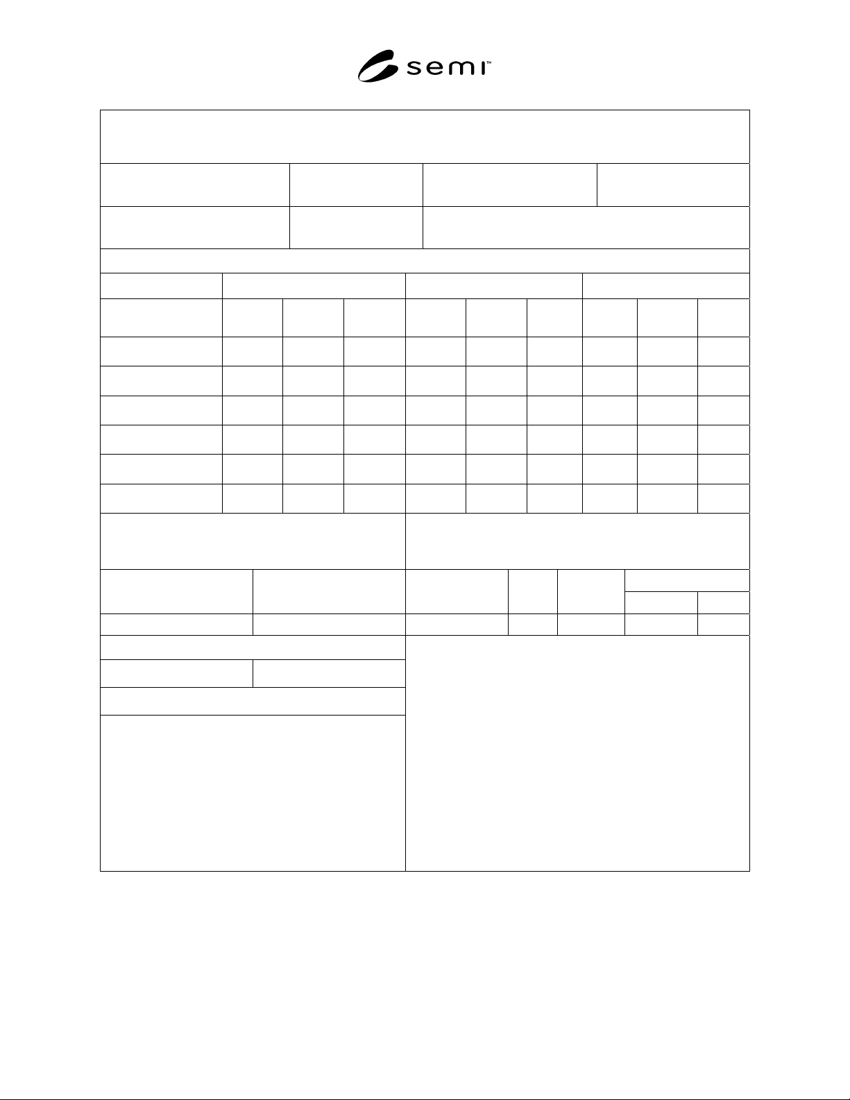
SEMI MF2166-0304 © SEMI 2004 8
Special Reference Wafer Calibration Data Sheet For
Non-Contact Dielectric Characterization System
System Supplier: System Model #:
System Software Rev: Test Date:
Calibration Organization
Operator ID Method A — Point Source Corona [ ]
Method B — Line Source Corona [ ]
Measurement Data Statistics
Mean
Std Dev (1 sigma) % Std Dev (1S%)
Location
Parameter
(0,0) (-40,40) (40,-40) (0,0) (-40,40)
(40,-40)
(0,0) (-40,40) (40,-40)
V
surf
(V) (Method A)
V
cpd,
(V) (Method B )
T
ox
(nm)
V
fb
(V)
Q
eff
(×10
11
charge/ cm
2
)
D
it
(×10
11
charge/ cm
2
)
Q
m
(× 10
11
charge/ cm
2
)
Environmental Data
Special Reference Wafer Used
Calibration Dates
Temperature
____ [ ]°F [ ]°C
Relative Humidity Serial Number Mfg.
Wafer
Dia.
Last Next
Equipment Performance Summary
In Tolerance [ ] Out of Tolerance [ ]
Repair Required Yes [ ] No [ ]
Comments
Figure 1
Example Data Sheet for Methods A and B