semi合集-English.pdf - 第7642页
SEMI T5-96 © SEMI 1996, 2004 5 8 Character Alignment 8.1 Char acter Skew — 3 degrees maximum allowable (see Figure 5). 8.2 Maxim u m character mi salignment (see Figures 6 and 7). 8.2.1 Maximum adjacent character misalig…
SEMI T5-96 © SEMI 1996, 2004 4
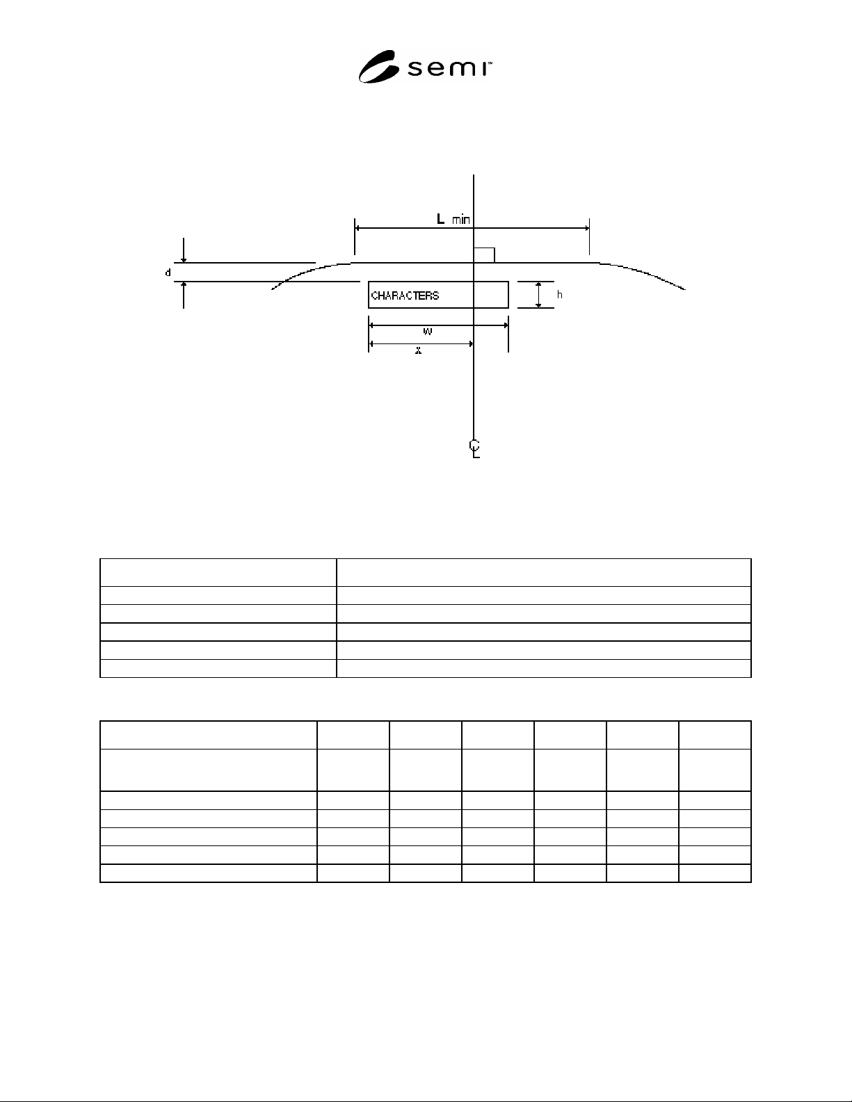
7.5 In the standard specification, the first character of the code line is located toward the left side of the code field.
Figure 4
Code Field Location for Flatted Wafers
Table 5 Location of Code Field
Wafer Diameter Location of Code Field
2" Front (standard); Back surface (alternate)
3" Front (standard); Back surface (alternate)
100 mm Front surface
125 mm Front surface
150 mm Front surface
Table 6 Code Field Location and Dimensions
Parameter (mm) 2" 3" 3" 100 mm 125 mm 150 mm
Configuration Character Dimension(See
Tables 1 and 2)
B B A
#1
A A A
L min 14.23 19.05 19.05 30.0 40.0 55.0
x 7.1 9.5 9.5 15.0 20.0 27.5
w 14.0 14.0 19.0 27.0 27.0 27.0
d 1.0 1.0 1.0 1.0 1.0 1.0
h 1.4 1.4 2.4 2.4 2.4 2.4
#1: For 3" wafers, only 13 characters are allowed due to limitations on the size of the code field.
SEMI T5-96 © SEMI 1996, 2004 5
8 Character Alignment
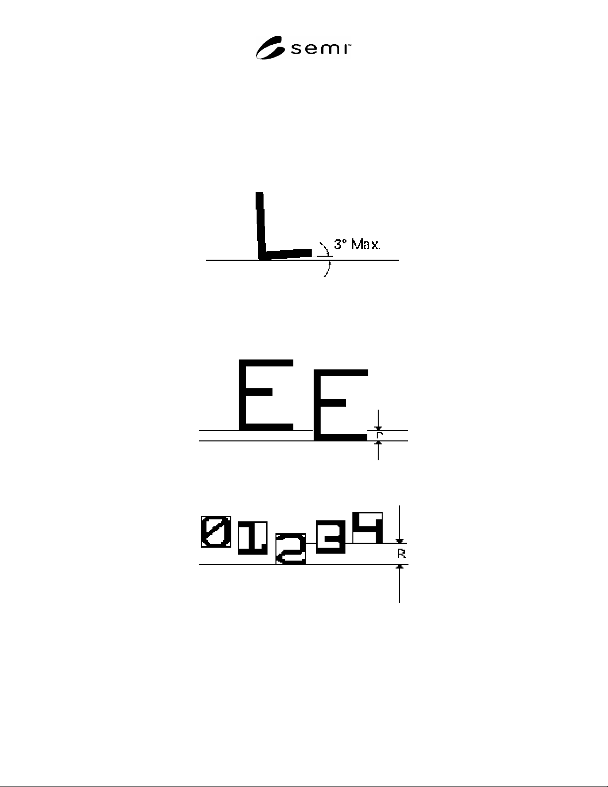
8.1 Character Skew — 3 degrees maximum allowable (see Figure 5).
8.2 Maximum character misalignment (see Figures 6 and 7).
8.2.1 Maximum adjacent character misalignment allowable is 0.230 mm.
8.2.2 Maximum line character misalignment allowable is 0.460 mm.
Figure 5
Character Skew
Figure 6
Adjacent Character Misalignment
Figure 7
Line Character Misalignment
SEMI T5-96 © SEMI 1996, 2004 6
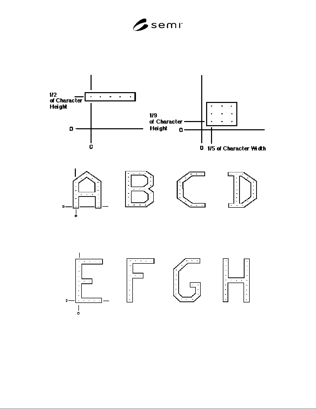
APPENDIX 1
SEMI OCR CHARACTER OUTLINES
NOTICE: The material in this appendix is an official part of SEMI T5 and was approved by full letter ballot procedures.