semi合集-English.pdf - 第792页
SEMI E106-1104 © SEMI 2000, 2004 10 I300I Guidelines on 30 0 mm Process Tool Mechanical Interfaces for Wafer Lot Deliv ery, Buffering, and Loading Integrated Mi nienvironmen t Design Best Practices
SEMI E106-1104 © SEMI 2000, 2004 9
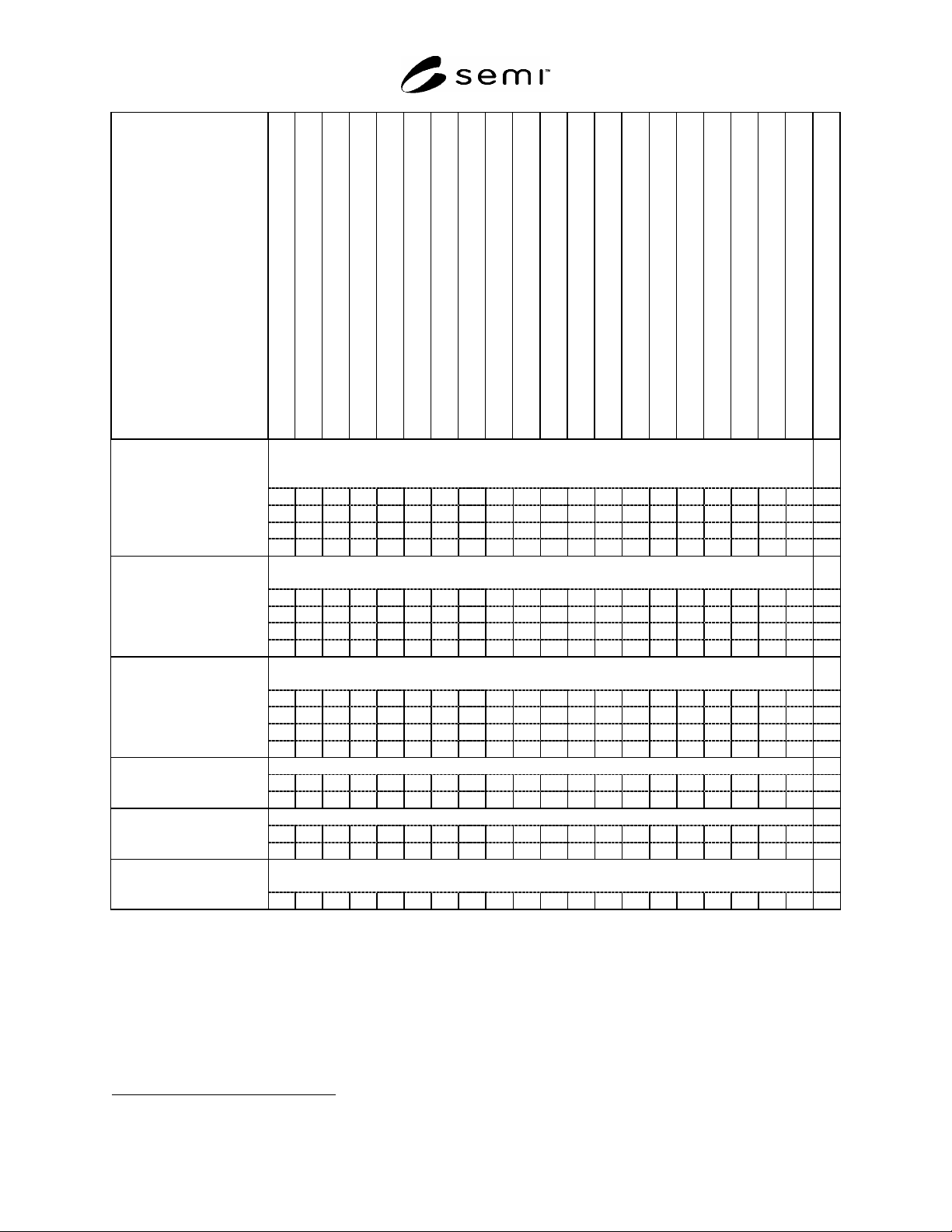
Type of Product and its
Components
SEMI M1.15, M8, or M28 (Wafer)
SEMI E57 (Kinematic Coupling)
SEMI E1.9 (Cassette)
SEMI E47.1 (FOUP)
SEMI M31 (FOSB)
SEMI E103 (Single-Wafer Box System)
SEMI E62 (FIMS)
SEMI E63 (BOLTS-M) and/or E92 (BOLTS-Light)
SEMI E15.1 (Load Port)
SEMI E64 (Cart Docking Interface)
SEMI E83 (PGV Docking Flange)
SEMI E84 (Carrier Handoff Parallel I/O)
SEMI E99 & E99.1 (Carrier ID Reader/Writer Comm.)
SEMI E85 (Stocker to Interbay Transport System)
SEMI E22.1 (Cluster- Tool End Effector)
SEMI E21.1 (Cluster-Tool Module Interface)
SEMI E25 & E26.1 (Cluster-Tool Access & Footprint)
SEMI E72 (Equipment Footprint, Height, and Weight)
SEMI G74 (Tape Frame)
SEMI G77 (Frame Cassette)
SEMI E110 (Indicator/Switch Placement)
main part of process
or metrology
equipment:
substrate handler I I D
box opener interface D
tool controller D
height and weight D
cluster tool central
handler module:
substrate handler I D
module interface D
footprint and access I
height and weight D
cluster tool process
module:
process chamber I I
module interface D
footprint and access D
height and weight D
wafer tape frame:
wafer contact I
other features D
frame cassette:
wafer/frame contact I I
other features D
back-end tool load
port:
carrier envelope I
8 Related Documents
1
Backend Global Joint Guidance for 300 mm Semiconductor Factories
Global Joint Guidance for 300 mm Semiconductor Factories
I300I Factory Guideline Compliance: Factory Integration Maturity Assessment for 300 mm Production Equipment
I300I Factory Guidelines
1 http://www.sematech.org/public/resources/300mm/guide.htm and http://www.sematech.org/public/resources/300mm/methods.htm

SEMI E106-1104 © SEMI 2000, 2004 10
I300I Guidelines on 300 mm Process Tool Mechanical Interfaces for Wafer Lot Delivery, Buffering, and Loading
Integrated Minienvironment Design Best Practices

SEMI E106-1104 © SEMI 2000, 2004 11
RELATED INFORMATION 1
NOTICE: This related information is not an official part of SEMI E106 and is not meant to modify or supersede it
in any way. Rather, these notes are provided primarily as a source of information to aid in the application of the
standard. As such, they are to be considered as reference material only. The standard should be referred to in all
cases.
R1-1 Standards Endorsed by Users — Section 8 lists documents in which the members of I300I and/or J300E have
endorsed SEMI 300 mm standards or have specified methods for testing compliance with those standards.
NOTICE: SEMI makes no warranties or representations as to the suitability of the standards set forth herein for any
particular application. The determination of the suitability of the standard is solely the responsibility of the user.
Users are cautioned to refer to manufacture's instructions, product labels, product data sheets, and other relevant
literature, respecting any materials or equipment mentioned herein. These standards are subject to change without
notice.
By publications of this standard, Semiconductor Equipment and Materials International (SEMI) takes no position
respecting the validity of any patent rights or copyrights asserted in connection with any items mentioned in this
standard. Users of this standard are expressly advised that determination of any such patent rights or copyrights, and
the risk of infringement of such rights are entirely their own responsibility.
Copyright by SEMI® (Semiconductor Equipment and Materials
International), 3081 Zanker Road, San Jose, CA 95134. Reproduction of
the contents in whole or in part is forbidden without express written
consent of SEMI.