semi合集-English.pdf - 第854页
SEMI E114-0302 E © SEMI 2002 8 Table 1 Example Data Table for Pr esenting the Test Methods Parameters Cable Length Test Instrument Parameters Model Number Bandwidth (Hz) Frequency (MHz) Test Method (1 or 2) Cable Assembl…
SEMI E114-0302
E
© SEMI 2002 7
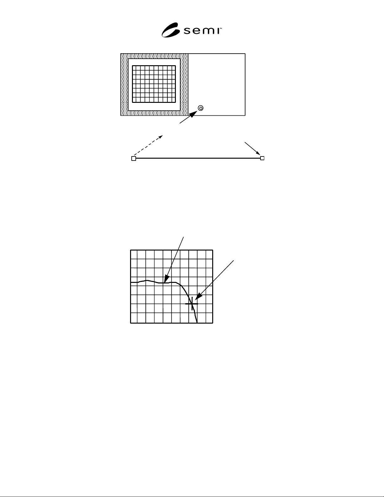
Short Circuit
Termination
Cable Assembly to be tested
Test Port
TDR
NOTE: The cable assembly to be tested (DUT) attaches to the test port and is terminated with a short circuit.
Figure 4
Schematic of the Time Domain Reflectometer (TDR) Test Setup for the Characteristic Impedance
Measurement
Point where impedance
is 45 ohms
50
45
40
55
60
Test Data Curve near
short circuit termination
Distance
Impedance
NOTE: The measurement termination point is defined as where the impedance at the short is equal to 0.9 times the nominal
impedance value, which would be 45 ohms for a 50-ohm nominal impedance.
Figure 5
Example Plot of the Characteristic Impedance of a 50-ohm Cable Assembly Near the Short Circuit
Termination
SEMI E114-0302
E
© SEMI 2002 8
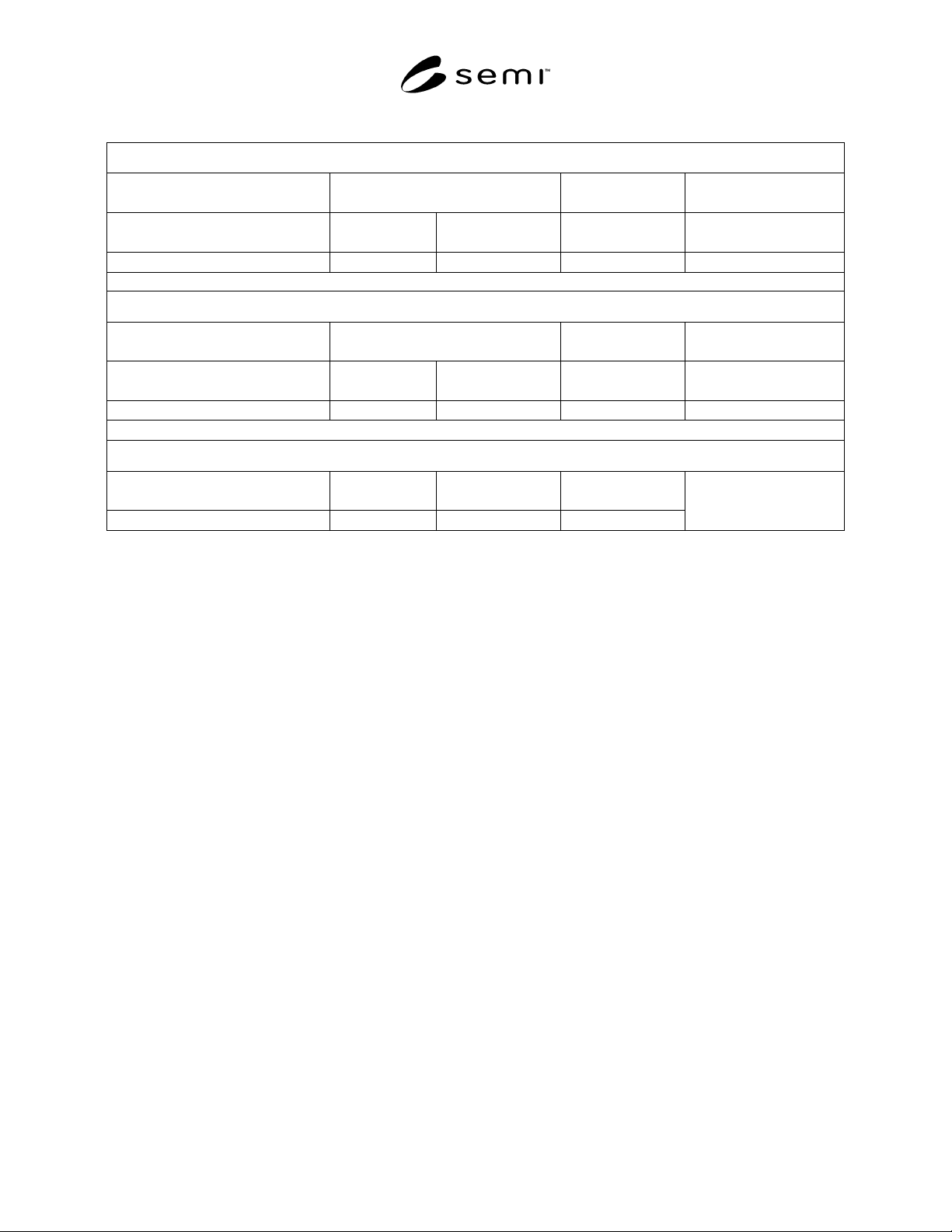
Table 1 Example Data Table for Presenting the Test Methods Parameters
Cable Length Test
Instrument
Parameters
Model Number
Bandwidth
(Hz)
Frequency (MHz) Test Method
(1 or 2)
Cable Assembly
Length (°)
Power Loss Test
Instrument
Parameters
Model Number
Bandwidth
(Hz)
Frequency (MHz) Loss (dB) Power Transferred (%)
Characteristic Impedance Test
Instrument
Model Number
Normalization
Factor
Minimum
Impedance
Maximum
Impedance
NOTICE: SEMI makes no warranties or representations as to the suitability of the standards set forth herein for any
particular application. The determination of the suitability of the standard is solely the responsibility of the user.
Users are cautioned to refer to manufacturer' s instructions, product labels, product data sheets, and other relevant
literature, respecting any materials or equipment mentioned herein. These standards are subject to change without
notice.
By publication of this standard, Semiconductor Equipment and Materials International (SEMI) takes no position
respecting the validity of any patent rights or copyrights asserted in connection with any items mentioned in this
standard. Users of this standard are expressly advised that determination of any such patent rights or copyrights, and
the risk of infringement of such rights are entirely their own responsibility.
Copyright by SEMI® (Semiconductor Equipment and Materials
International), 3081 Zanker Road, San Jose, CA 95134. Reproduction o
f
the contents in whole or in part is forbidden without express writte
n
consent of SEMI.

SEMI E115-0302
E
© SEMI 2002 1
SEMI E115-0302
E
TEST METHOD FOR DETERMINING THE LOAD IMPEDANCE AND
EFFICIENCY OF MATCHING NETWORKS USED IN SEMICONDUCTOR
PROCESSING EQUIPMENT RF POWER DELIVERY SYSTEMS
This test method was technically approved by the Global Metrics Committee and is the direct responsibility
of the North American Metrics Committee. Current edition approved by the North American Regional
Standards Committee on March 30, 2002. Initially available at www.semi.org June 2002; to be published
July 2002. Previously published March 2002.
E
This document was editorially modified in May 2002 to correct an errata. A change was made in Section
1.1.
1 Purpose
1.1 The purpose of this document is to define a test
method used to determine the load impedance and
efficiency of matching networks used in RF power
delivery systems for semiconductor processing
equipment.
2 Scope
2.1 This document specifies the testing procedures and
test equipment required for determining the load
impedance and power efficiency of a matching network
based on the positions of the tuning elements in the
matching network.
2.2 The primary focus for this specification is
semiconductor processing equipment including, but not
limited to, the following tool types:
• Dry etch equipment,
• Film deposition equipment (CVD and PVD).
2.3 This standard does not address any safety or
performance issues related to RF emissions or electrical
codes (e.g., Underwriter’s Laboratory, Inc. (UL), the
National Electrical Code (NEC
), Federal
Communications Commission (FCC)). It is the
responsibility of the users of this standard to conform to
the appropriate local codes and regulations as applied to
this type of equipment, some of which are covered by
referenced documents.
2.4 This standard does not purport to address safety
issues, if any, associated with its use. It is the
responsibility of the users of this standard to establish
appropriate safety and health practices and determine
the applicability of regulatory limitations prior to use.
3 Limitations
3.1 This standard addresses RF Matching Networks
used in RF systems that primarily operate in the
frequency range of 0.2–100 MHz. It does not address
higher frequency RF systems or microwave systems.
3.2 This standard is meant for analyzing matching
networks that are designed to operate at fixed frequency
with a 50-ohm input impedance.
3.3 International, national, and local codes, regulations
and laws should be consulted to ensure that the
equipment and procedures meet regulatory
requirements in each location.
4 Referenced Standards
4.1 SEMI Standards
SEMI E113 — Specification for Semiconductor
Processing Equipment RF Power Delivery Systems
4.2 IEEE Standards
1
IEEE-STD-383 — IEEE Standard for Type Test of
Class 1E Electrical Cables, Field Splices, and
Connections for Nuclear Power Generating Stations
4.3 Military Standards
2
MIL-PRF-39012D — General Specification for
Connectors, Coaxial, Radio Frequency
5 Terminology
5.1 Abbreviations and Acronyms
5.1.1 CVD — Chemical Vapor Deposition
5.1.2 PVD — Physical Vapor Deposition
5.1.3 VSWR — Voltage Standing Wave Ratio
5.2 Definitions of Terms
5.2.1 complex conjugate load impedance — the
complex conjugate load impedance has the same real
part of the load impedance and the negative of the
reactive part of the load impedance. For example, the
1 Institute of Electrical and Electronics Engineers, IEEE Operations
Center, 445 Hoes Lane, P.O. Box 1331, Piscataway, New Jersey
08855-1331, USA. Telephone: 732.981.0060; Fax: 732.981.1721
2 Available through the Naval Publications and Forms Center, 5801
Tabor Avenue, Philadelphia, PA 19120-5099, USA. Telephone:
215.697.3321