semi合集-English.pdf - 第928页
SEMI E118.1-1104 © SEMI 2003, 2004 5 RELATED INFORMATION 1 SCENARIOS NOTICE: This rela ted inform ation is not an o fficial part of SEMI E118. 1 and was derive d from the work of the originating task force. Th is related…
SEMI E118.1-1104 © SEMI 2003, 2004 4
8.3 2D Code Read Condition Attributes
8.3.1 Table 6 specifies the values for the 2D Code Read Condition attribute identifiers and limitations on values.
Table 6 2D Code Read Condition Attribute Definitions
Attribute Name Description Access Format Value
Optional
“CellSize” Number of Pixels in a Cell RO 20 “000”–“999”
“Contrast” Contrast Percentage of Dark / Light RO 20 “000”–“100”
“Damage Percent” Percentage of Damage Cell RO 20 “000”–“100”
“Number Error Bits” Number of the Damage Cell RO 20 “000”–“999”
“Read Time” Time for Readout, in seconds RO 20 “000”–“120”
“Matrix Style” Normal Mode or Mirror Mode RO 20 “NO” = Normal Mode
“MR” = Mirror Mode
“Matrix Polarity” Dark on Light or Light on Dark RO 20 “DON” = Dark on Light
“LON” = Light on Dark
To show that data is not available for an attribute, the attribute value is set to a zero-length string.
Note 1: A zero-length item for an attribute value means that does not exist.
NOTICE: SEMI makes no warranties or representations as to the suitability of the standards set forth herein for any
particular application. The determination of the suitability of the standard is solely the responsibility of the user.
Users are cautioned to refer to manufacturer's instructions, product labels, product data sheets, and other relevant
literature, respecting any materials or equipment mentioned herein. These standards are subject to change without
notice.
By publication of this standard, Semiconductor Equipment and Materials International (SEMI) takes no position
respecting the validity of any patent rights or copyrights asserted in connection with any items mentioned in this
standard. Users of this standard are expressly advised that determination of any such patent rights or copyrights, and
the risk of infringement of such rights are entirely their own responsibility.
SEMI E118.1-1104 © SEMI 2003, 2004 5
RELATED INFORMATION 1
SCENARIOS
NOTICE: This related information is not an official part of SEMI E118.1 and was derived from the work of the
originating task force. This related information was approved for publication by full letter ballot procedures on
January 10, 2003.
This section provides examples of typical scenarios for a Wafer ID Reader.
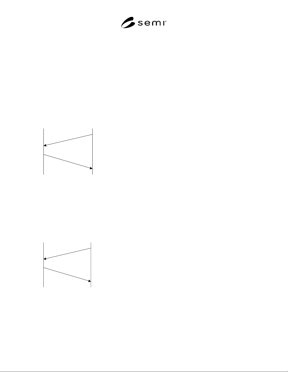
R1-1 Read WID
R1-1.1 The upstream controller sends a Read WID
Request message to the WIDR for Head 1. The WIDR
Head 1 reads the ID, and the WIDR returns the ID to
the upstream controller.
WIDR
Upstream
Controller
S18, F9 Read ID Request
Target ID = “01”
S18, F10 Read ID Data
MID = “XYZ001”
Figure R1-1
Read WID Scenario
R1-2 Read WID
R1-2.1 The upstream controller sends a Read WID
Request message to the WIDR for Head 1. The WIDR
Head 1 reads the ID, but the WIDR can't read the ID.
There isn't the ID on the wafer.
WIDR
Upstream
Controller
S18, F9 Read ID Request
Target ID = “01”
S18, F10 Read ID Data
Rsult Status = “EE”
MID = “”
Figure R1-2
Read WID Scenario
NOTICE: SEMI makes no warranties or
representations as to the suitability of the standards set
forth herein for any particular application. The
determination of the suitability of the standard is solely
the responsibility of the user. Users are cautioned to
refer to manufacturer's instructions, product labels,
product data sheets, and other relevant literature,
respecting any materials or equipment mentioned
herein. These standards are subject to change without
notice.
By publication of this standard, Semiconductor
Equipment and Materials International (SEMI) takes no
position respecting the validity of any patent rights or
copyrights asserted in connection with any items
mentioned in this standard. Users of this standard are
expressly advised that determination of any such patent
rights or copyrights, and the risk of infringement of
such rights are entirely their own responsibility.
Copyright by SEMI® (Semiconductor Equipment and Materials
International), 3081 Zanker Road, San Jose, CA 95134. Reproduction of
the contents in whole or in part is forbidden without express written
consent of SEMI.
SEMI E119-1104 © SEMI 2002, 2004 1
SEMI E119-1104
MECHANICAL SPECIFICATION FOR REDUCED-PITCH FRONT-
OPENING BOX FOR INTERFACTORY TRANSPORT OF 300 mm
WAFERS
This specification was technically approved by the Global Physical Interfaces and Carriers Committee and is
the direct responsibility of the North American Physical Interfaces and Carriers Committee. Current edition
approved by the North American Regional Standards Committee on August 16, 2004. Initially available at
www.semi.org September 2004; to be published November 2004. Originally published November 2002.
1 Purpose
1.1 This standard partially specifies a reduced-pitch
front-opening box for interfactory transport of 300 mm
wafers (FOBIT). This reduced-pitch box, with a
capacity of 25 wafers but with the approximate physical
volume of a 13-wafer FOUP, is intended to reduce the
cost of transporting wafers between IC manufacturing
sites. To leverage current industry 300 mm technology,
this reduced-pitch front-opening box is intended to
interface with 13-wafer FIMS, as specified in SEMI
E62.
2 Scope
2.1 This standard is intended to set an appropriate level
of specification that places minimal limits on
innovation while ensuring modularity and inter-
changeability at all mechanical interfaces. Only the
physical interfaces for FOBIT are specified; no
materials requirements or micro-contamination limits
are given. However, this standard has been written so
that both metal and injection-molded plastic FOBITs
can be manufactured in conformance with it.
2.2 This standard assumes that the FOBIT is intended
for use in the interfactory transportation of wafers. The
following boundary conditions were used in the
creation of this specification:
Minimizing the pitch between wafers will reduce
the cost of transporting wafers.
The FOBIT will be used for interfactory
transportation of both processed and unprocessed
wafers.
The box will have a 25-wafer capacity.
Random access of wafers, using edge grip handling
devices, is not a requirement for this standard.
The FOBIT will be compatible with the following
300 mm Standards:
13-wafer FIMS Interface (SEMI E62)
300 mm Load Port (SEMI E15.1)
Kinematic Coupling (SEMI E57)
The FOBIT will not necessarily be compliant with
the following 300 mm Standards due to wafer
restraint requirements and product applications
during transportation:
300 mm Front-Opening Unified Pod (SEMI E47.1)
300 mm Open Cassette (SEMI E1.9)
300 mm Front-Opening Shipping Box (SEMI
M31)
The technical requirements of this standard are
written for the transportation of nominal thickness
wafers, as defined by SEMI M1.15.
2.3 This reduced-pitch, 25-capacity FOBIT is designed
for use with the 13-capacity FIMS interface, as
specified in SEMI E62.
NOTICE: This standard does not purport to address
safety issues, if any, associated with its use. It is the
responsibility of the users of this standard to establish
appropriate safety and health practices and determine
the applicability of regulatory or other limitations prior
to use.
3 Referenced Standards
3.1 SEMI Standards
SEMI E1.9 — Mechanical Specification for Cassettes
Used to Transport and Store 300 mm Wafers
SEMI E15 — Specification for Tool Load Port
SEMI E15.1 — Specification for 300 mm Tool Load
Port
SEMI E47.1 — Provisional Mechanical Specification
for Boxes and Pods Used to Transport and Store 300
mm Wafers
SEMI E57 — Mechanical Specification for Kinematic
Couplings Used to Align and Support 300 mm Wafer
Carriers
SEMI E62 — Provisional Specification for 300 mm
Front-Opening Interface Mechanical Standard (FIMS)