MIL- STD-883F 2004 TEST METHOD STANDARD MICROCIRCUITS.pdf - 第128页
MIL-STD-883F METHOD 1019.6 7 March 2003 12 This page i ntenti onally lef t blank
MIL-STD-883F
METHOD 1019.6
7 March 2003
11
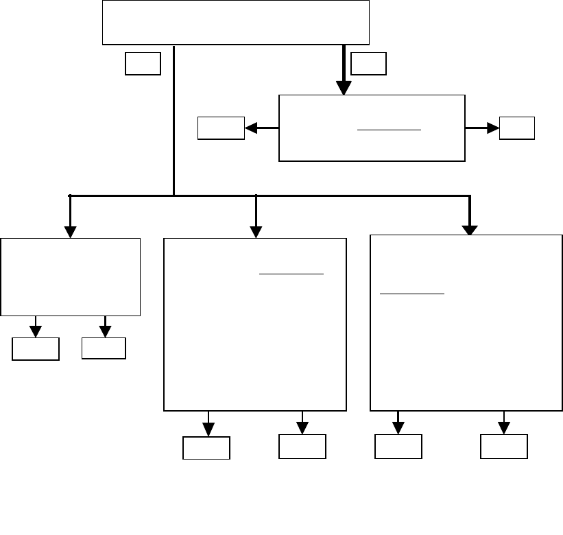
Figure 1019-
2. Flow diagram for ionizing radiation test procedure for bipolar (or BiCMOS) linear
or mixed-signal circuits
Determine the need for ELDRS testing
See Para. 3.13
No
Yes
Perform standard test
(Para 3.6.1 Condition A)
See Para 3.13.1
Pass Fail
Test at the intended
application dose rate
Para 3.6.3
Condition C
Perform low dose rate test
per Para 3.6.4, Condition D
1. ≤ 25 krad:
≤ 10 mrad/s
dose = 1.5 spec
2. >25 krad:
≥ 1000 hrs
dose = 2 spec
Perform elevated temperature
irradiation per Para 3.6.5,
Condition E
1. May be used if spec dose
≤ 50 krad
2. 0.5 to 5 rad/s, 100 ° C
3. Parameter design margin = 3
Pass
Pass
Fail
Pass Fail Fail
MIL-STD-883F
METHOD 1019.6
7 March 2003
12
This page intentionally left blank

MIL-STD-883F
METHOD 1020.1
15 November 1991
1
METHOD 1020.1
DOSE RATE INDUCED LATCHUP TEST PROCEDURE
1. PURPOSE
. This test procedure defines the detailed requirements for performing latchup testing of microcircuits to
identify susceptibility to dose rate induced latchup.
1.1 Definitions
. Definitions of terms used in this procedure are provided below:
a. Dose rate induced latchup. Dose rate induced latchup is regenerative device action in which a parasitic region
(e.g., a four layer p-n-p-n or n-p-n-p path) is turned on by a photocurrent generated by a pulse of ionizing
radiation, and remains on for an indefinite period of time after the photocurrent subsides. The device will remain
latched as long as the power supply delivers voltage greater than the holding voltage and current greater than the
holding current. Latchup disrupts normal circuit operation in some portion of the circuit, and may also cause
catastrophic failure due to local heating of semiconductor regions, metallization or bond wires.
b. Latchup windows. A latchup window is the phenomenon in which a device exhibits latchup in a specific range of
dose rates. Above and below this range, the device does not latchup. A device may exhibit more than one
latchup window. This phenomenon has been observed for some CMOS logic devices, oxide sidewall logic and
LSI memories, and may occur in other devices.
c. Combinational logic. Combinational (determined) logic devices are those whose output is solely determined by
the logic signals at its inputs (except for switching delays). Combinational logic circuits contain no internal storage
elements, and include multiplexers, decoders, and gates.
d. Sequential logic. Sequential (nondetermined) devices are those in which the output state at any given time
depends on the sequence and time relationship of logic signals that were previously applied to its inputs.
Sequential logic circuits contain internal storage elements. Examples of sequential logic devices are shift
registers, memories, counters, and flip-flops.
e. Recovery period. The recovery period is the time interval in which the device supply current recovers from the
radiation pulse.
f. Holding voltage and holding current: The voltage and current above which latchup is sustained.
1.2 Test plan
. Prior to latchup testing, a latchup test plan shall be prepared which describes the radiation source, the
dosimetry techniques, test equipment and conditions to be used. A detailed procedure for each device type to be tested
shall be prepared, either as part of the test plan or in separate test procedure documents. The procedure shall include bias
conditions, test sequence, and schematics of the test setup. The test plan shall be approved by the acquiring activity, and
as a minimum, the items listed below shall be provided in the test plan or test procedure:
a. Device types, including package types, and quantities to be tested.
b. Traceability requirements, such as requirements for serialization, wafer or lot traceability, etc.
c. Requirements for data reporting and submission.
d. Temperature for test (see 2.3.6).
e. Block diagram or schematic representation of test set up.
f. Electrical parameters to be monitored and device operating conditions, including bias conditions and functional
test requirements before, during, and after the radiation pulse.
g. Group A electrical test requirements for pre- and post-latchup testing, to include test limits and failure criteria.