MIL- STD-883F 2004 TEST METHOD STANDARD MICROCIRCUITS.pdf - 第136页
MIL-STD-883F METHOD 1020.1 15 November 1991 8 3.5.2. 4 Other devic e types . For ot her types of mic roci rcui ts, such as LSI/VLSI and greater complexity c irc uits and hybrid micr ocir cuit s, t he worst case bi as c o…

MIL-STD-883F
METHOD 1020.1
15 November 1991
7
Step 14: Change the conditions of the initial output to the complement state and repeat steps 10-13. (The number of
states in which the device is to be tested shall be specified in the test plan or procedure.)
Step 15: Remove bias voltages and device, in that order.
In sequential logic devices, the radiation pulse can cause logic state changes at the output as well as within internal storage
registers. Therefore, the post-radiation verification of recovery must be determined from a combination of device supply
current and post-exposure functional test results. A sequential logic device fails the latchup test if the supply current does
not return to within specified limits within the specified recovery period or if it fails the functional test requirements. The
specified supply current limits must take into account changes in the supply current that may result from changes in the
internal logic state and internal registers.
3.5.2.3 Linear devices
. Latchup testing for linear devices is inherently device and application specific because of the
large number of types of linear circuits and application conditions. Latchup in linear devices is detected through a
combination of monitoring the device supply current, monitoring of the output waveform, and in-situ functional tests. The
minimum number of monitored outputs shall be as specified in the test plan or procedure, but the in-situ functional test shall
exercise all outputs. The transient response of the device output is monitored through the use of an oscilloscope with a
camera, or a transient digitizer. An example is shown on figure 1020-2. Trace A shows a device output which operated
properly after the radiation pulse, and trace B shows an output that failed. Note that the device will not respond properly to
the oscillating input after the radiation exposure. Testing of linear devices is performed as follows:
Step 8: Install the DUT in the proper position in front of the radiation source, and bring the device up to test
temperature.
Step 9: Bias the device in accordance with the test plan or procedure and verify proper device functional operation.
Step 10: Adjust input signal as specified in the test plan or procedure and verify correct output level.
Step 11: Irradiate the device and record the dose. Monitor the supply current and output voltages during and after
the pulse, and measure the recovery times of the supply current and the output voltages. Monitor the
waveform of the output.
Step 12: After the recovery period, determine if the device supply currents have returned to within the specified limits.
Step 13: Determine if the output voltages have returned to within specified limits in the specified recovery time.
Ensure device responds properly to input commands, and compare pre-rad and post-rad waveforms.
Step 14: Change the conditions of the input as specified in the test plan or procedure and repeat steps 10-13. (The
number of conditions in which the device is to be tested shall be specified in the test plan or procedure.)
Step 15: Remove the bias voltages and device, in that order.
A linear device fails the latchup test if the supply current or the output signals (or voltages) do not recover within the
recovery period specified in the test plan, or if the outputs do not respond properly to an input signal.

MIL-STD-883F
METHOD 1020.1
15 November 1991
8
3.5.2.4 Other device types
. For other types of microcircuits, such as LSI/VLSI and greater complexity circuits and hybrid
microcircuits, the worst case bias conditions, exposure states, outputs to be monitored, necessary post-irradiation testing,
and failure criteria are determined through a combination of characterization testing and analysis. These requirements are
specified in the test plan or procedure for each device. Depending on the circuit type, the device is tested as described in
3.5.2.1 to 3.5.2.3.
4. REPORT
. A latchup test report shall be prepared in which the devices tested are identified by device type,
manufacturer, date code, and lot/wafer identification. The report shall list by device serial number, pass/fail status of each
device and the doses (or dose range) delivered to each device in each radiation pulse. The test plan and procedure shall
either be appended to the test report or referenced in the test report.
5. SUMMARY
. The following details shall be specified in the applicable acquisition document:
a. Device types and quantities to be tested.
b. Temperature of test (see 2.3.6).
c. Traceability (device number, wafer/lot number, etc.) requirements and requirements for data reporting and
submission.
d. The maximum allowable recovery period.
e. Radiation pulse width and radiation dose per pulse.
f. Total dose limit for each device type.
g. Requirements for group A electrical testing pre- and post-latchup testing.
h. Test instrument requirements, if other than those indicated above.
i. Requirements for characterization, recharacterization, and analysis.
j. Minimum dc power supply current required, or value of current limiting resistor, if allowed.
MIL-STD-883F
METHOD 1020.1
15 November 1991
9
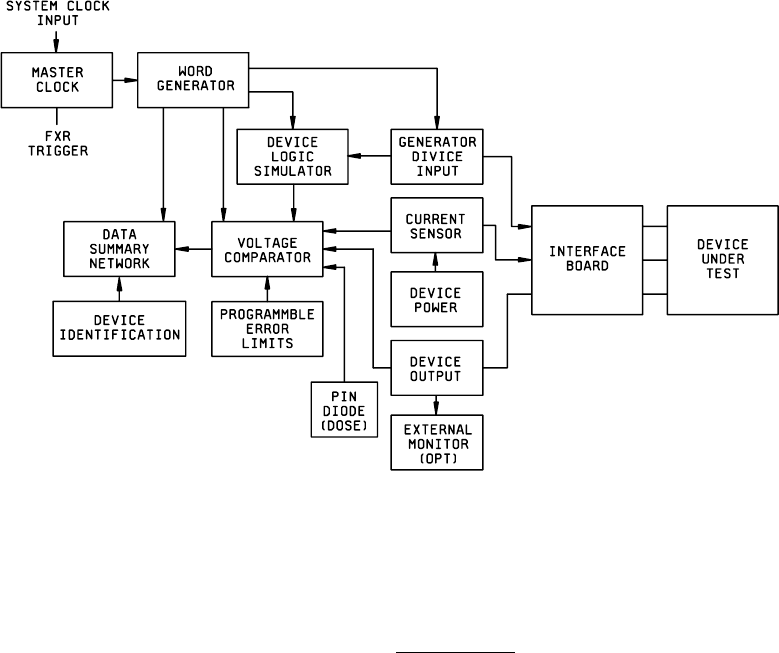
FIGURE 1020-1. Latchup system
.