MIL- STD-883F 2004 TEST METHOD STANDARD MICROCIRCUITS.pdf - 第139页
MIL-STD-883F METHOD 1021.2 15 November 1991 1 METHOD 1021.2 DOSE RATE UPSET TESTING OF DIGITAL MI CROCIRCUITS 1. PURPOSE . This test procedur e defines the requi rements for t esti ng the res ponse of pac kaged di gital …
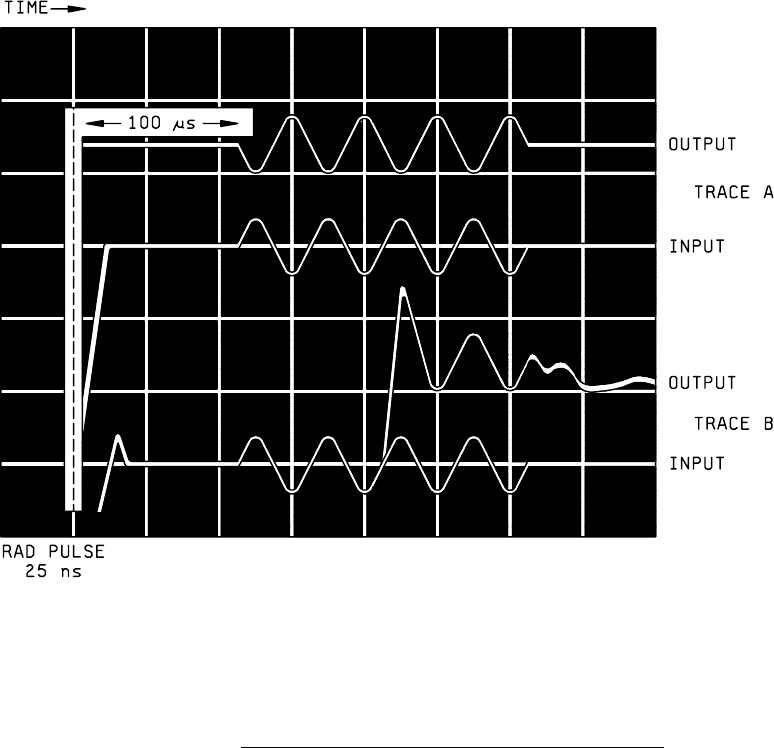
MIL-STD-883F
METHOD 1020.1
15 November 1991
10
FIGURE 1020-2. Linear device latchup screen test photograph (50 µs/div)
.

MIL-STD-883F
METHOD 1021.2
15 November 1991
1
METHOD 1021.2
DOSE RATE UPSET TESTING OF DIGITAL MICROCIRCUITS
1. PURPOSE
. This test procedure defines the requirements for testing the response of packaged digital integrated
circuits to pulsed ionizing radiation. A flash x-ray or linear accelerator is used as a source of pulses of ionizing radiation.
The response may include transient output signals, changes in the state of internal storage elements, and transient current
surges at inputs, outputs, and power supply connections. The dose rate at which logic or change-of-state errors first occur
is of particular interest in many applications.
1.1 Definitions
. Definitions of terms used in this procedure are given below:
a. Dose rate threshold for upset. The dose rate which causes either:
(1) A transient output upset for which the change in output voltage of an operating digital integrated circuit goes
either above or below (as appropriate) specified logic levels (see 3.2 on transient voltage criteria), and the
circuit spontaneously recovers to its preirradiation condition after the radiation pulse subsides, or
(2) A stored data or logic state upset for which there is a change in the state of one or more internal memory or
logic elements that does not
recover spontaneously after the radiation pulse. However, the circuit can be
restored to its preirradiation condition by applying the same sequence of logic signals to its inputs that were
previously used to establish the preirradiation condition, or
(3) A dynamic upset which results in a change in the expected output or stored test pattern of a device that is
functionally operating during the time it is irradiated. The upset response may depend on the precise time
relationship between the radiation pulse and the operating cycle of the device. For operations requiring
many clock signals, it may be necessary to use a wide radiation pulse.
b. Dose rate. Energy absorbed per unit time per unit mass by a given material from the radiation field to which it is
exposed.
c. Combinational logic circuit. A digital logic circuit with the property that its output state is solely determined by the
logic signals at its inputs. Combinational logic circuits contain no internal storage elements. Examples of
combinational circuits include gates, multiplexers, and decoders.
d. Sequential logic circuit. A digital logic circuit with the property that its output state at a given time depends on the
sequence and time relationship of logic signals that were previously applied to its inputs. Sequential logic circuits
contain internal storage elements. Examples of sequential logic circuits include memories, shift registers,
counters, and flip-flops.
e. State vector. A state vector completely specifies the logic condition of all elements within a logic circuit. For
combinational circuits the state vector includes the logic signals that are applied to all inputs; for sequential
circuits the state vector must also include the sequence and time relationship of all input signals (this may include
many clock cycles).

MIL-STD-883F
METHOD 1021.2
15 November 1991
2
1.2 Interferences
. There are several interferences that need to be considered when this test procedure is applied. These
include:
a. Total dose damage. Devices may be permanently damaged by total dose. This limits the number of radiation
pulses that can be applied during transient upset testing. The total dose sensitivity depends on fabrication
techniques and device technology. MOS devices are especially sensitive to total dose damage. Newer bipolar
devices with oxide-isolated sidewalls may also be affected by low levels of total dose. The maximum total dose to
which devices are exposed must not exceed 20 percent of the typical total dose failure level of the specific part
type.
b. Steps between successive radiation levels. The size of the steps between successive radiation levels limits the
accuracy with which the dose rate upset threshold is determined. Cost considerations and total dose damage
limit the number of radiation levels that can be used to test a particular device.
c. Latchup. Some types of integrated circuits may be driven into a latchup condition by transient radiation. If latchup
occurs, the device will not function properly until power is temporarily removed and reapplied. Permanent damage
may also occur, primarily due to the large amount of localized heating that results. Although latchup is an
important transient response mechanism, this procedure does not apply to devices in which latchup occurs.
Functional testing after irradiation is required to detect internal changes of state, and this will also detect latchup.
However, if latchup occurs it will usually not be possible to restore normal operation without first interrupting the
power supply.
d. Limited number of state vectors. Cost, testing time, and total dose damage usually make it necessary to restrict
upset testing to a small number of state vectors. These state vectors must include the most sensitive conditions
in order to avoid misleading results. An analysis is required to select the state vectors used for radiation testing to
make sure that circuit and geometrical factors that affect the upset response are taken into account (see 3.1).
2. APPARATUS
. Before testing can be done, the state vectors must be selected for radiation testing. This requires a
logic diagram of the test device. The apparatus used for testing shall consist of the radiation source, dosimetry equipment,
a test circuit board, line drivers, cables, and electrical test instrumentation to measure the transient response, provide bias,
and perform functional tests. Adequate precautions shall be observed to obtain an electrical measurement system with
ample shielding, satisfactory grounding, and low noise from electrical interference or from the radiation environment.
2.1 Radiation source
. The radiation source used in this test shall be either a flash x-ray machine (FXR) used in the
photon mode or a linear accelerator (LINAC) used in the electron beam mode. The LINAC beam energy shall be greater
than 10 MeV. The radiation source shall provide a uniform (within 20 percent) radiation level across the area where the
device and the dosimeter will be placed. The radiation pulse width for narrow pulse measurements shall be between 10 and
50 ns. For narrow pulse measurements either a LINAC or FXR may be used. Wide pulse measurements (typically 1 - 10
µs) shall be performed with a LINAC. The pulse width for LINAC irradiations shall be specified. The dose rate at the
location of the device under test shall be adjustable between 10
6
and 10
12
rads(Si)/s (or as required) for narrow pulse
measurements and between 10
5
and 10
11
rads(Si)/s (or as required) for wide pulse measurements. Unless otherwise
specified, a test device exposed to a total dose that exceeds 20 percent of the total dose failure level shall be considered as
destructively tested and shall be removed from the lot (see 1.2a).
2.2 Dosimetry equipment
. Dosimetry equipment must include a system for measuring total dose, such as a
thermoluminescent dosimeter (TLD) or calorimeter, a pulse shape monitor, and an active dosimeter that allows the dose rate
to be determined from electronic measurements, e.g., a p-i-n detector, Faraday cup, secondary emission monitor, or current
transformer.