MIL- STD-883F 2004 TEST METHOD STANDARD MICROCIRCUITS.pdf - 第192页
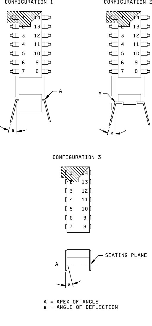
MIL-STD-883F METHOD 2004.5 29 November 1985 6 FIGURE 2004-1 Angl e of bend for dual -in- line pac kage c onfigurat ions .

MIL-STD-883F
METHOD 2004.5
29 November 1985
5
3.1 Failure criteria
. The device shall be considered a failure if any of the following occurs:
a. The stud breaks or is elongated greater than one-half of the thread pitch.
b. It fails the specified post-test end point measurements.
c. There is evidence of thread stripping or deformation of the mounting seat.
4. SUMMARY
. The following details shall be specified in the applicable acquisition document:
a. The amount of torque to be applied (see 3).
b. Length of time torque is to be applied (see 3).
c. Measurements to be made after test (see 3).
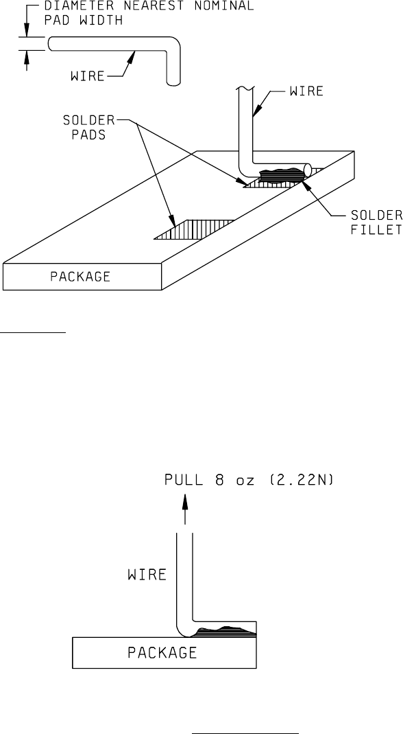
TEST CONDITION D - SOLDER PAD ADHESION FOR LEADLESS CHIP CARRIER AND SIMILAR DEVICES
1. PURPOSE
. This test is designed to check the capabilities of the device solder pads to withstand a delamination (peel)
stress of specified tension and time.
2. APPARATUS
. Equipment for 10X magnification, suitable clamps and fixtures for securing the device and applying the
specified tension/time conditions to wires soldered to the device solder pads. Equivalent linear pull test equipment may be
used.
3. PROCEDURE
. Unless otherwise specified, a delamination (peel) stress test shall be applied to randomly selected
solder pads from each device selected for test. Further, unless otherwise specified, the sampling shall be Sample Size
Number = 15, c = 0 based on the number of solder pads tested, chosen from a minimum of three devices. Preparation and
testing of devices shall be in accordance with figure 2004-2 of this method and as follows.
a. Pretinned soft annealed solid copper wire of a gauge (diameter) nearest, but not exceeding that of the nominal
solder pad width, shall be soldered using Sn60A or Pb40A or Sn63A or Pb37A of ANSI/J-STD-006 (previously
known as Sn60 or Sn63 solder in accordance with QQ-S-571) to each solder pad to be tested in a manner such
that the wire is bonded over the entire solder pad length and terminates at the package edge (see figure 2004-2).
The unsoldered portion of the wire shall be bent perpendicular to the bond plane prior to attachment. Caution
should be taken to assure that the solder pad metallization is not damaged during the soldering or the wire
bending operation.
b. Unless otherwise specified, a minimum tension of 8 ounces (2.22 N) shall be applied, without shock, to each
solder pad to be tested in a direction perpendicular to the solder pad surface and maintained for 30 seconds
minimum.
3.1 Failure criteria
. When examined, using 10X magnification, after removal of the tension stress, the appearance of any
delamination involving constituent solder pad interfaces shall be considered an adhesion failure of the solder pad.
Separation of the solder pad from the device is an obvious (without visual magnification) adhesion failure. Separation of the
wire from the solder fillet (leaving the solder pad intact) or wire breakage is considered a test procedure failure.
4. SUMMARY
. The following details shall be specified in the applicable acquisition document:
a. Sampling criteria, if other than specified (see 3.1).
b. Failure criteria, if other than specified (see 3.1).
c. Tension to be applied in this test if other than 8 ounces (2.22 N).
d. Length of time tension is to be applied if other than 30 seconds.
MIL-STD-883F
METHOD 2004.5
29 November 1985
6
FIGURE 2004-1 Angle of bend for dual-in-line package configurations
.
MIL-STD-883F
METHOD 2004.5
29 November 1985
7
MATERIALS
Flux: Flux type symbol “A” or “B” (flux type “L0” or “L1”)
in accordance with ANSI/J-STD-004 (previously
designated as Type R or RMA only, in accordance
with MIL-F-14256).
Solder: Sn60A or Pb40A or Sn63A or Pb37A in accordance
with ANSI/J-STD-006 (previously designated as
Sn 60 or Sn 63 in accordance with QQ-S-571).
Wire: Soft annealed solid copper.
FIGURE 2004-2 Solder pad adhesion
.