MIL- STD-883F 2004 TEST METHOD STANDARD MICROCIRCUITS.pdf - 第210页
MIL-STD-883F METHOD 2009.9 19 August 1994 8 This page i ntenti onally lef t blank
MIL-STD-883F
METHOD 2009.9
19 August 1994
7
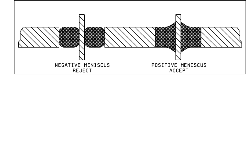
FIGURE 2009-9. Reentrant seals
.
4. SUMMARY
. The following details shall be specified in the applicable acquisition document:
a. Requirements for markings and the lead (terminal), or pin identification.
b. Any additional detailed requirements for materials, design, construction, and workmanship.
MIL-STD-883F
METHOD 2009.9
19 August 1994
8
This page intentionally left blank
MIL-STD-883F
METHOD 2010.11
18 June 2004
1
METHOD 2010.11
INTERNAL VISUAL (MONOLITHIC)
1. PURPOSE
. The purpose of this test is to check the internal materials, construction, and workmanship of microcircuits
for compliance with the requirements of the applicable acquisition document. This test will normally be used prior to capping
or encapsulation on a 100 percent inspection basis to detect and eliminate devices with internal defects, that could lead to
device failure in normal applications. It may also be employed on a sampling basis prior to capping to determine the
effectiveness of the manufacturer's quality control and handling procedures for microelectronic devices. Furthermore, the
criteria of this test method will be used during destructive physical analysis (DPA) following the procedures outlined in test
method 5009, "Destructive Physical Analysis". Test condition A and B provide a rigorous and detailed procedure for internal
visual inspection of high reliability microcircuits as specified in the screening requirements of test method 5004. For
condition B product the alternate screening procedure (alternate 1) documented in test method 5004 may be used by the
manufacturer as an option to internal visual inspection as specified. For condition A or B product, the alternate screening
procedure (alternate 2) documented in test method 5004 may be used by the manufacture as an option to internal visual
inspection as specified.
2. APPARATUS
. The apparatus for this test shall include optical equipment capable of the specified magnification and
any visual standards (gauges, drawings, photographs, etc.) necessary to perform an effective examination and enable the
operator to make objective decisions as to the acceptability of the device being examined. Adequate fixturing shall be
provided for handling devices during examination to promote efficient operation without inflicting damage to the units.
2.1 GaAs device requirements
. GaAs devices shall be inspected to all applicable criteria as listed herein. GaAs
microwave devices shall also have additional specific criteria as listed and the applicable high power magnification for
individual features of GaAs microwave devices shall be selected from the following table.
TABLE I. GaAs microwave device high magnification requirements
.
Feature Dimensions Magnification range
> 5 microns 75 - 150x
1 - 5 microns 150 - 400x
< 1 micron 400 - 1000x
2.2 Silicon-on-Sapphire (SOS) device requirements
. SOS devices shall be inspected to all applicable criteria specified
herein, except where noted. The sapphire portions of the die shall be considered "nonconductive and nonoperational
material".
3. PROCEDURE
.
a. General. The device shall be examined within the specified magnification range to determine compliance with the
requirements of the applicable acquisition document and the criteria of the specified test condition.
The inspections and criteria in this method shall be required inspections for all devices and locations to which they
are applicable. Where the criterion is intended for a specific device process or technology, it has been indicated.
*