MIL- STD-883F 2004 TEST METHOD STANDARD MICROCIRCUITS.pdf - 第218页
MIL-STD-883F METHOD 2010.11 18 June 2004 8 Condition A Conditi on B Class le vel S Class lev el B FIGURE 2010-5. Metalli zation s crat ch cr iter ia for c lass level B . b. For condit ion A, s ee 3.1.1.1a above. b. For c…
MIL-STD-883F
METHOD 2010.11
18 June 2004
7
NOTE: The piece part audit requirements can be replaced by a piece part cleaning process, approved by the qualifying
activity, that is always performed either prior to or during the assembly process and these piece parts are stored in a
controlled environment until they are used.
The intent of these procedures is to require investigation and resolution of foreign material problems that do not
have an effective screening or detection methodology but that could cause degradation and eventual failure of the
device function. Repetitive findings without obvious improvements require escalation to Director of Manufacturing
and Director of Quality Assurance to continue processing.
Condition A Condition B
Class level S Class level B
3.1 High power inspection
. Internal visual examination as required in 3.1.1 through 3.1.3 shall be conducted on each
microcircuit. In addition, the applicable criteria contained in 3.1.4 through 3.1.7 shall be used for the appropriate microcircuit
area where glassivation, dielectric isolation or film resistors are used.
NOTE: Unless otherwise specified, for flip chip product the criteria of 3.1 shall apply only to top circuit side inspection. After
die mounting, only criteria in 3.1.3i shall apply.
The high magnification The high magnification
inspection shall be within the inspection shall be within the
range of 100X to 200X. range of 75X to 150X.
For high magnification inspection of GaAs microwave devices, see table I herein. Also, for < 1 micron features, the
manufacturer may implement a sample inspection plan which shall be documented in the manufacturer's internal procedure
and approved by the qualifying activity.
3.1.1 Metallization defects
. No device shall be acceptable that exhibits the following defects in the operating
metallization.
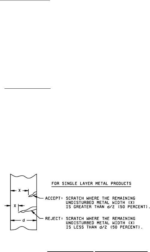
3.1.1.1 Metallization scratches:
a. Scratch in the metallization excluding a. Scratch in the metallization, excluding bonding
bonding pads and beam leads that leaves pads and beam leads, that exposes underlying
less than 50 percent of the original passivation anywhere along its length and leaves
metal width undisturbed (see figure less than 50 percent of the original metal width
2010-4). undisturbed (see figure 2010-5).
NOTE: For GaAs microwave devices, scratches in the gate stripe or gate insertion metallization.
FIGURE 2010-4. Metallization scratch
criteria for class level S.
MIL-STD-883F
METHOD 2010.11
18 June 2004
8
Condition A Condition B
Class level S Class level B
FIGURE 2010-5. Metallization scratch criteria for class level B
.
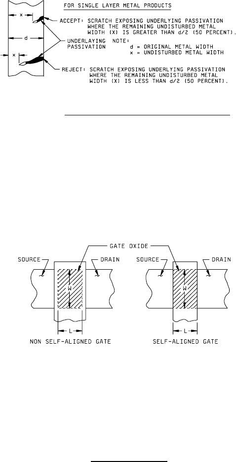
b. For condition A, see 3.1.1.1a above. b. For condition B only. Scratch that completely
crosses a metallization path and damages the
surface of the surrounding passivation, glassivation,
or substrate on either side (for MOS devices, the
path shall be the (L) dimension) (see figure 2010-6).
NOTE: When standard metallization scratch criterion
is applied to the gate area, the dimensions (W) and (L)
shall be considered as the original channel width and
length respectively.
FIGURE 2010-6. MOS scratch criteria
.
MIL-STD-883F
METHOD 2010.11
18 June 2004
9
Condition A Condition B
Class level S Class level B
FIGURE 2010-6. MOS scratch criteria
- Continued.
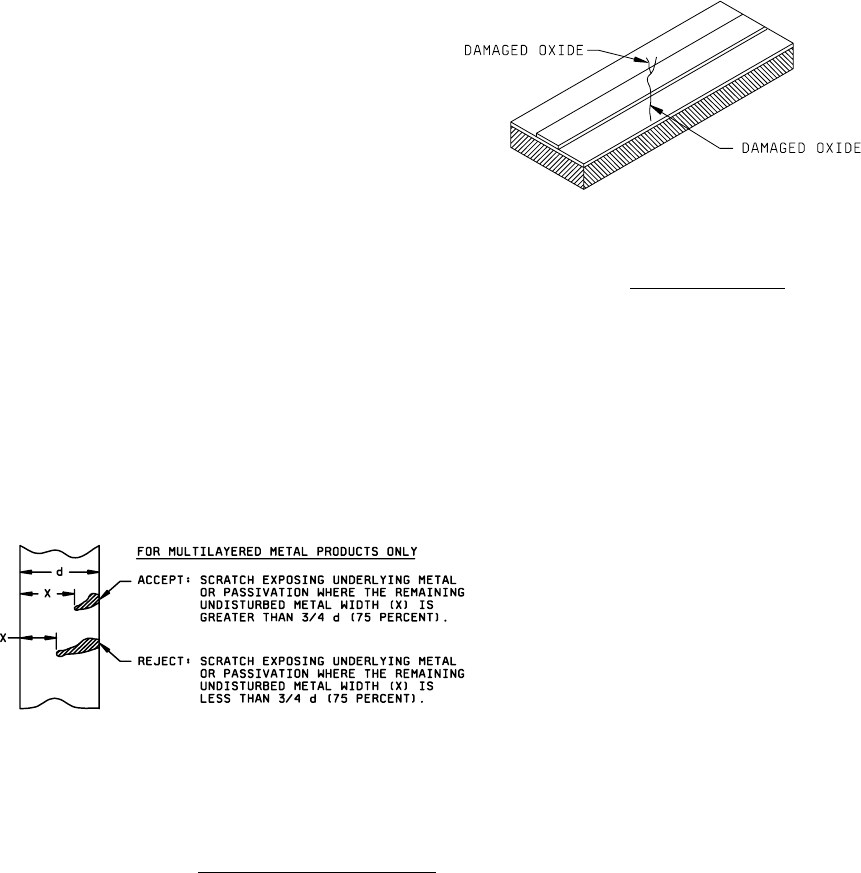
c. Scratch in multilayered metallization, excluding c. Scratch in multilayered metallization, excluding
bonding pads and beam leads that exposes bond pads and beam leads that exposes the
underlying metal or passivation anywhere underlying metal anywhere along its length
along its length and leaves less than 75 and leaves less than 25 percent of the original
percent of the original metal width metal width undisturbed (see figure 2010-8).
undisturbed (see figure 2010-7).
FIGURE 2010-7. Scratch criteria for class level S
.