MIL- STD-883F 2004 TEST METHOD STANDARD MICROCIRCUITS.pdf - 第222页
MIL-STD-883F METHOD 2010.11 18 June 2004 12 Condition A Conditi on B Class le vel S Class lev el B FIGURE 2010-10. MOS scr atch c riter ia for clas s level S . FIGURE 2010- 11. MOS sc ratc h crit eria f or clas s level B…
MIL-STD-883F
METHOD 2010.11
18 June 2004
11
Condition A Condition B
Class level S Class level B
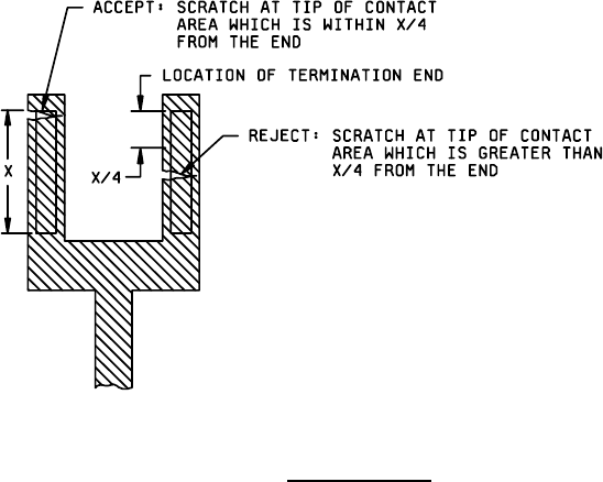
FIGURE 2010-9. Termination ends
.
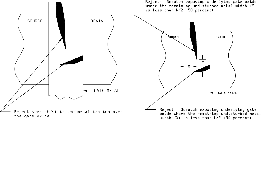
e. Scratch in the metallization, over the e. Scratch in the metallization, over the
gate oxide (applicable to MOS structures gate oxide, that exposes underlying
only) (see figure 2010-10). passivation and leaves less than 50 percent
of the length or width of the metallization
between source and drain diffusion undisturbed
(applicable to MOS structures only) (see figure
2010-11).
MIL-STD-883F
METHOD 2010.11
18 June 2004
12
Condition A Condition B
Class level S Class level B
FIGURE 2010-10. MOS scratch criteria for class level S
. FIGURE 2010-11. MOS scratch criteria for class level B.
MIL-STD-883F
METHOD 2010.11
18 June 2004
13
Condition A Condition B
Class level S Class level B
f. Scratch in the metallization that exposes the dielectric material of a thin film capacitor or crossover. (Not
applicable to air bridges.)
g. Scratch in the bonding pad or fillet area that g. Scratch in the bonding pad or fillet area that
reduces the metallization path width connecting exposes underlying passivation or substrate
the bond to the interconnecting metallization and reduces the metallization path width
to less than 50 percent of the narrowest connecting the bond to the interconnecting
entering interconnect metallization stripe metallization to less than 50 percent of the
width. If two or more stripes enter a bonding narrowest entering interconnect metallization
pad, each shall be considered separately. stripe width. If two or more stripes enter
a bonding pad, each shall be considered
separately.
h. Scratch(es) (probe mark(s), etc.) in the bonding pad area that exposes underlying passivation or substrate and
leaves less than 75 percent of the unglassivated metallization area undisturbed.
i. For GaAs devices only, any tears, peeling, gaps, and lateral displacement of metal.
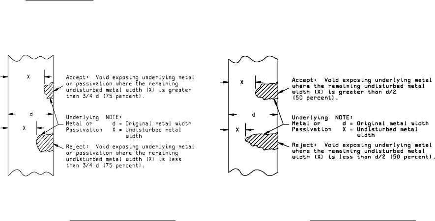
3.1.1.2 Metallization voids
;
a. Void(s) in the metallization that leaves less than a. Void(s) in the metallization that leaves less than
75 percent of the original metal width undisturbed 50 percent of the original metal width undisturbed
(see figure 2010-12). (see figure 2010-13).
FIGURE 2010-12. Void criteria for class level S
. FIGURE 2010-13. Void criteria for class level B.
NOTE: For condition B only. Criteria can be excluded
for peripheral power or ground metallization where
parallel paths exist so that an open at the void(s) would
not cause an unintended isolation of the metallization
path.