MIL- STD-883F 2004 TEST METHOD STANDARD MICROCIRCUITS.pdf - 第225页
MIL-STD-883F METHOD 2010.11 18 June 2004 15 Condition A Conditi on B Class le vel S Class lev el B d. Voi d(s) that l eave less than 75 perc ent of t he d. Voi d(s) that l eave less than 60 perc ent of t he metalliza tio…
MIL-STD-883F
METHOD 2010.11
18 June 2004
14
Condition A Condition B
Class level S Class level B
b. Void(s) in the metallization over a passivation step that leaves less than 75 percent of the original metal width at
the step undisturbed.
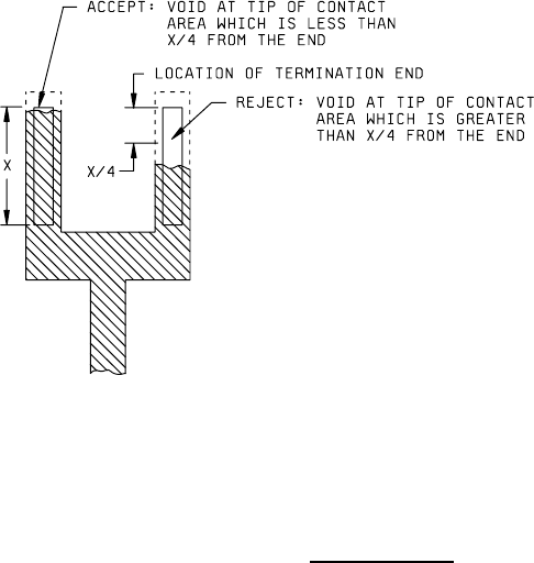
NOTE: For condition B only. Criteria of 3.1.1.2a and b
can be excluded for the last 25 percent of the linear
length of the contact cut and all metal beyond on the
termination end(s) of metallization runs. In these cases
there shall be at least 50 percent of the contact opening
perimeter covered by undisturbed metallization (see
figure 2010-14).
FIGURE 2010-14. Termination ends
.
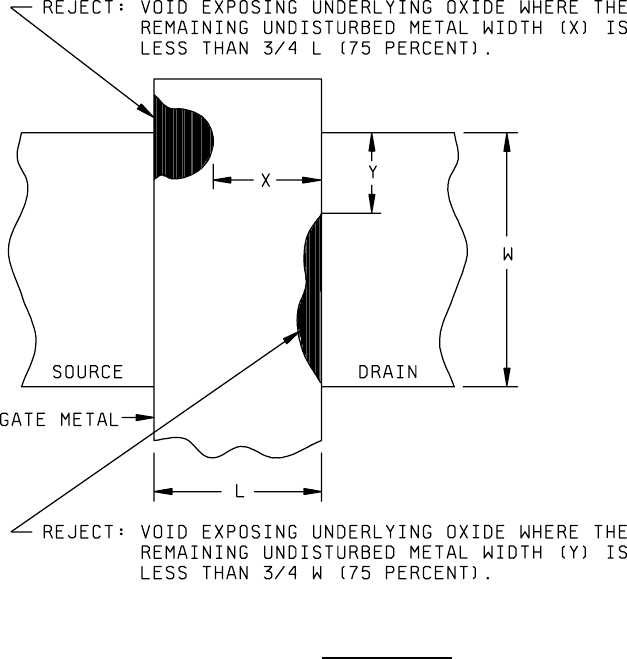
c. Void(s) in the metallization over the gate oxide that leaves less than 75 percent of the metallization length (L) or
width (W) between source and drain diffusions undisturbed (applicable to MOS structures only) (see figure
2010-15).
MIL-STD-883F
METHOD 2010.11
18 June 2004
15
Condition A Condition B
Class level S Class level B
d. Void(s) that leave less than 75 percent of the d. Void(s) that leave less than 60 percent of the
metallization area over the gate oxide undisturbed metallization area over the gate oxide undisturbed
(applicable to MOS structures only). (applicable to MOS structures only).
e. Void(s) that leaves less than 75 percent of the metallization width coincident with the source or drain diffusion
junction line undisturbed (applicable to MOS structures only) (see figure 2010-15).
FIGURE 2010-15. MOS void criteria
.
f. Void(s) in the bonding pad area that leaves less than 75 percent of its original unglassivated metallization area
undisturbed (see figure 2010-16).
g. Void(s) in the bonding pad or fillet area that reduces g. Void(s) in the bonding pad or fillet area that
the metallization path width connecting the bond to reduces the metallization path width connecting
the interconnecting metallization to less than 75 the bond to the interconnecting metallization
percent of the narrowest entering metallization stripe to less than 50 percent of the narrowest entering
width. If two or more stripes enter a bonding pad, metallization stripe width. If two or more
each shall be considered separately. (see figure stripes enter a bonding pad, each shall be
2010-16). considered separately (see figure 2010-16).
MIL-STD-883F
METHOD 2010.11
18 June 2004
16
Condition A Condition B
Class level S Class level B
FIGURE 2010-16. Bond pad terminology
.
NOTE: When a fillet area exists, it is to be considered as part of the entering/exiting metallization stripe.
h. Void(s) in the metallization area of a thin film capacitor that leave less than 75 percent of the designed
metallization area.
i. For GaAs microwave devices only, voids in the gate stripe.
3.1.1.3 Metallization corrosion
. Any metallization corrosion. Metallization having any localized discolored area shall be
closely examined and rejected, unless it is demonstrated to be a harmless film, glassivation interface, or other obscuring
effect.
3.1.1.4 Metallization nonadherence
. Any metallization lifting, peeling, or blistering.
3.1.1.5 Metallization probing
. Criteria contained in 3.1.1.1 shall apply as limitations on probing damage.