MIL- STD-883F 2004 TEST METHOD STANDARD MICROCIRCUITS.pdf - 第232页
MIL-STD-883F METHOD 2010.11 18 June 2004 22 Condition A Conditi on B Class le vel S Class lev el B 3.1.2. 2 Passi vation f aults . NOTE: For SOS devi ces, exclude defec ts bet ween fir st- level c onductive i nterc onnec…
MIL-STD-883F
METHOD 2010.11
18 June 2004
21
Condition A Condition B
Class level S Class level B
3.1.2 Diffusion and passivation layer faults
. No devices shall be acceptable that exhibits the following:
3.1.2.1 Diffusion faults
.
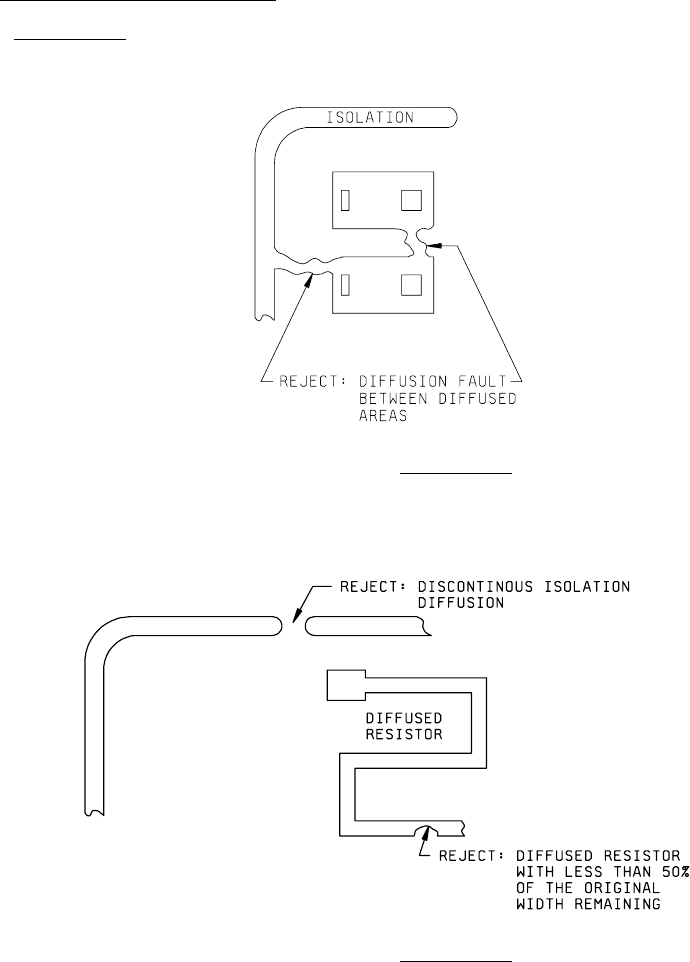
a. Diffusion fault that allows bridging between diffused areas (see figure 2010-19).
FIGURE 2010-19. Diffusion faults
.
b. Any isolation diffusion that is discontinuous (except isolation walls around unused areas or unused bonding pads)
or any other diffused area with less than 25 percent (50 percent for resistors) of the original diffusion width
remaining (see figure 2010-20).
FIGURE 2010-20. Diffusion faults
.
MIL-STD-883F
METHOD 2010.11
18 June 2004
22
Condition A Condition B
Class level S Class level B
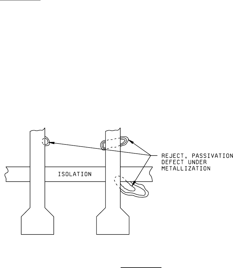
3.1.2.2 Passivation faults
.
NOTE: For SOS devices, exclude defects between first-level conductive interconnect (metallization, polysilicon, ect.) and
sapphire areas of the die, where no active circuit elements are present.
a. Either multiple lines or a complete absence of passivation visible at the edge and continuing under the
metallization unless by design for GaAs devices. Multiple lines indicate that the fault can have sufficient depth to
penetrate down to bare semiconductor material.
NOTE: The multiple line criteria can be excluded when a second passivation layer is applied in a separate operation
prior to metallization deposition or for bond pads located in isolated tubs.
NOTE: For condition B only. Should the absence
of glassivation in the defect area or the
characteristics of the glassivation present
allow verification of the presence or absence of
passivation by color or color comparisons
respectively, then these techniques may be used
(see figure 2010-21).
FIGURE 2010-21. Passivation faults
.
b. Active junction line not covered by passivation, unless by design.
c. Contact window that extends across a junction line, unless by design.

MIL-STD-883F
METHOD 2010.11
18 June 2004
23
Condition A Condition B
Class level S Class level B
3.1.3 Scribing and die defects
. No device shall be acceptable that exhibits:
a. Less than 0.25 mil of passivation visible a. No line of separation between operating
between operating metallization or bond metallization or bond periphery and bare
periphery and bare semiconductor material semiconductor material (see figure 2010-22).
(see figure 2010-22).
NOTE: For GaAs devices only, less than 0.1 mil of substrate visible between operating metallization or bond periphery
and edge of the die.
NOTE: Criteria can be excluded for beam leads and peripheral metallization including bonding pads where the
metallization is at the same potential as the substrate.
NOTE: Does not apply to SOS devices.
b. A chipout or crack in the active circuit area (see figures 2010-22 and 2010-38). In addition for GaAs a chipout into
or underneath the functional metallization, e.g., bond pads, capacitors, peripheral metallization, etc., but excluding
test structures of the device.
NOTE: Criteria can be excluded for peripheral metallization that is at the same potential as the substrate. At least 50
percent undisturbed metallization width shall remain at the chipout.
c. A crack that exceeds 3.0 mils in length, or c. A crack that exceed 5.0 mils in length, or
comes closer than 0.25 mils to any operating that does not exhibit a line of separation to
metallization (except for substrate potential any operating metallization (except for
peripheral metal) or functional circuit element substrate potential peripheral metal) or
(see figure 2010-22). function circuit element (see figure 2010-22).
d. For condition A only. Semicircular crack(s) d. No condition B.
terminating at the die edge, whose chord is long
enough to bridge the narrowest spacing between
unglassivated operating material (e.g.,
metallization, bare semiconductor material,
mounting material, bonding wire, etc.) (see figure
2010-22).
e. Exposed semiconductor material extending over the passivation edge at the point of the beam lead exit from the
die (applicable to beam lead structures only) (see figure 2010-38).
f. Die having attached portions of the active circuit area of another die.
g. A crack that exceeds 1.0 mil in length inside the scribe line (or semiconductor material edge for beam lead
devices) that points toward operating metallization or functional circuit elements (see figure 2010-22).
h. A crack that comes closer than 0.5 mil to operating beam lead metallization (see figure 2010-38).
NOTE: Criteria of 3.1.3c and h can be excluded for beam lead devices where the chipout or crack does not extend
into the semiconductor material.
NOTE: Criteria of 3.1.3e and h do not apply to GaAs devices.