MIL- STD-883F 2004 TEST METHOD STANDARD MICROCIRCUITS.pdf - 第235页
MIL-STD-883F METHOD 2010.11 18 June 2004 25 Condition A Conditi on B Class le vel S Class lev el B i. For flip chip , cracks, or chi pouts in the s ubstr ate mater ial that extends beyond 50 perc ent of s ubst rate thi c…
MIL-STD-883F
METHOD 2010.11
18 June 2004
24
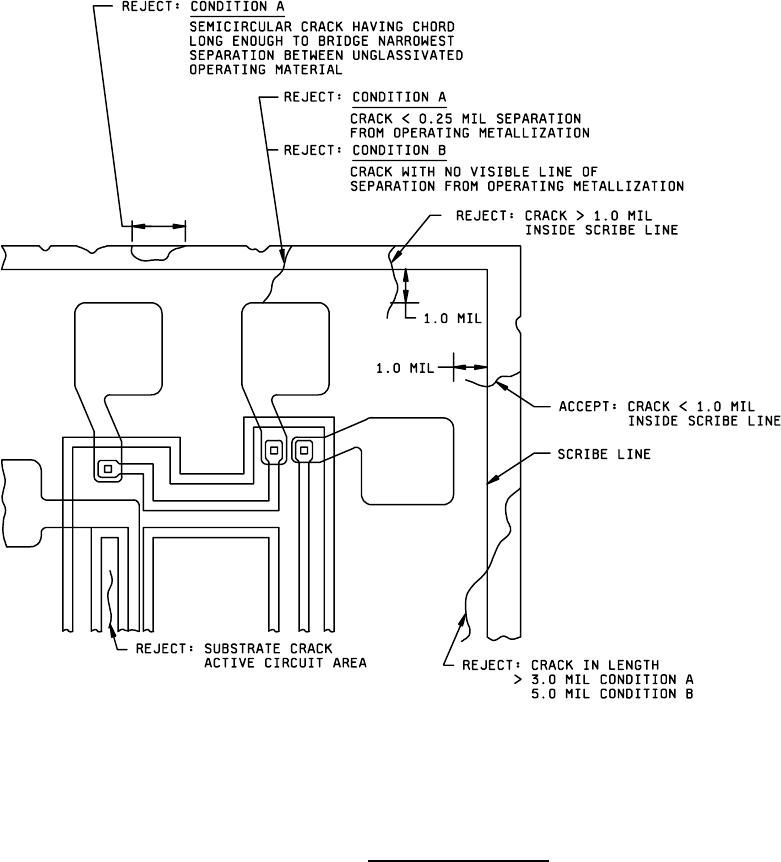
FIGURE 2010-22 Scribing and die defects.
MIL-STD-883F
METHOD 2010.11
18 June 2004
25
Condition A Condition B
Class level S Class level B
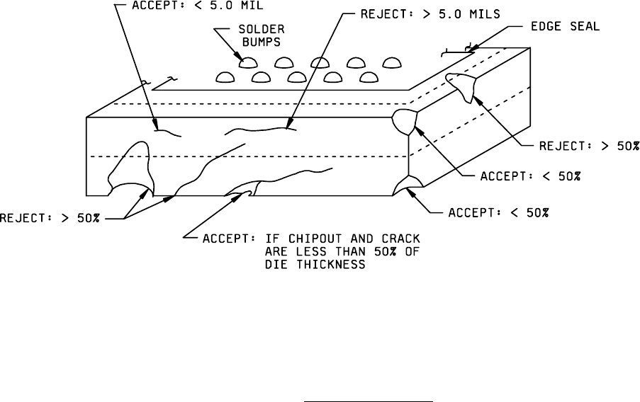
i. For flip chip, cracks, or chipouts in the substrate material that extends beyond 50 percent of substrate thickness
or a crack greater than 5.0 mils in length in the substrate material (see figure 2010-23).
FIGURE 2010-23. Scribing and die defects
.
j. Any blistering, peeling, delamination, corrosion, or other gross defects in glassivation, metal, interlevel dielectrics
or other layers.
MIL-STD-883F
METHOD 2010.11
18 June 2004
26
Condition A Condition B
Class level S Class level B
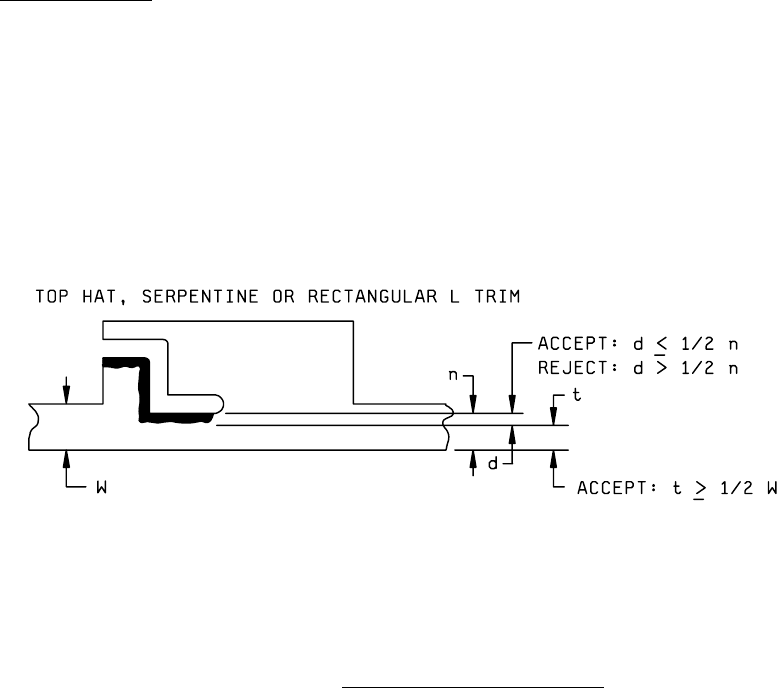
3.1.4 Glassivation defects
. No device shall be acceptable that exhibits (see figure 2010-24):
NOTE: For condition B only. Criteria of 3.1.4 can be
excluded when the defect(s) is due to laser trimming. In
this case, the defects outside the kerf due to laser
trimming shall not be more than one half the remaining
resistor width and shall leave a primary resistor path
free of glassivation defects, equal to or greater than one
half times the narrowest resistor width.
FIGURE 2010-24. Laser trimmed glassivation defects
.
a. Glass crazing or glass damage that prohibits the detection of visual criteria contained herein.
b. Any lifting or peeling of the glassivation in the active areas or which extends more than 1.0 mil distance from the
designed periphery of the glassivation.
c. A glassivation void that exposes two or more active metallization paths, except by design.
d. Unglassivated areas greater than 5.0 mils in any dimension, unless by design.
e. Unglassivated areas at the edge of bonding pad exposing bare semiconductor material, except by design.
f. Glassivation covering more than 25 percent of the designed open contact bonding area.
g. Crazing over a film resistor.