MIL- STD-883F 2004 TEST METHOD STANDARD MICROCIRCUITS.pdf - 第239页
MIL-STD-883F METHOD 2010.11 18 June 2004 29 Condition A Conditi on B Class le vel S Class lev el B a. Any mi sali gnment between t he conduct or/r esis tor i n which t he actual width X of t he overlap i s les s than 50 …
MIL-STD-883F
METHOD 2010.11
18 June 2004
28
Condition A Condition B
Class level S Class level B
c. A diffused area which overlaps dielectric isolation material and does not exhibit a line of separation to an adjacent
tub, or an overlap of more than one diffusion area into the dielectric isolation material (see figure 2010-25).
FIGURE 2010-26. Dielectric isolation defects
.
d. A contact window that touches or overlaps dielectric material, except by design.
NOTE: Metallization scratch and void defects over a dielectric isolation step shall be rejected in accordance with
criteria contained in 3.1.1.1d and 3.1.1.2b.
3.1.6 Film resistor
. Rejection shall be based on defects found within the actively used portions of the film resistor.
Metallization defect criteria of 3.1.1 shall apply as applicable. No device shall be acceptable that exhibits:
MIL-STD-883F
METHOD 2010.11
18 June 2004
29
Condition A Condition B
Class level S Class level B
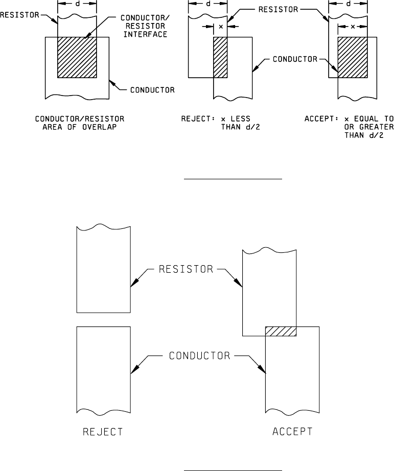
a. Any misalignment between the conductor/resistor in which the actual width X of the overlap is less than 50
percent of the original resistor width.
FIGURE 2010-27. Film resistor contact area
.
b. No visible line of contact overlap between the metallization and film resistor (see figure 2010-28).
FIGURE 2010-28. Film resistor contact area
.
MIL-STD-883F
METHOD 2010.11
18 June 2004
30
Condition A Condition B
Class level S Class level B
c. Void or necking down that leaves less than 75 percent of the film resistor width undisturbed at a terminal.
d. Inactive resistor inadvertently connected to two separate points on an active circuit.
e. Separation between any two resistors or a resistor and a metallization path that is less than 0.25 mil, or 50
percent of the design separation, whichever is less.
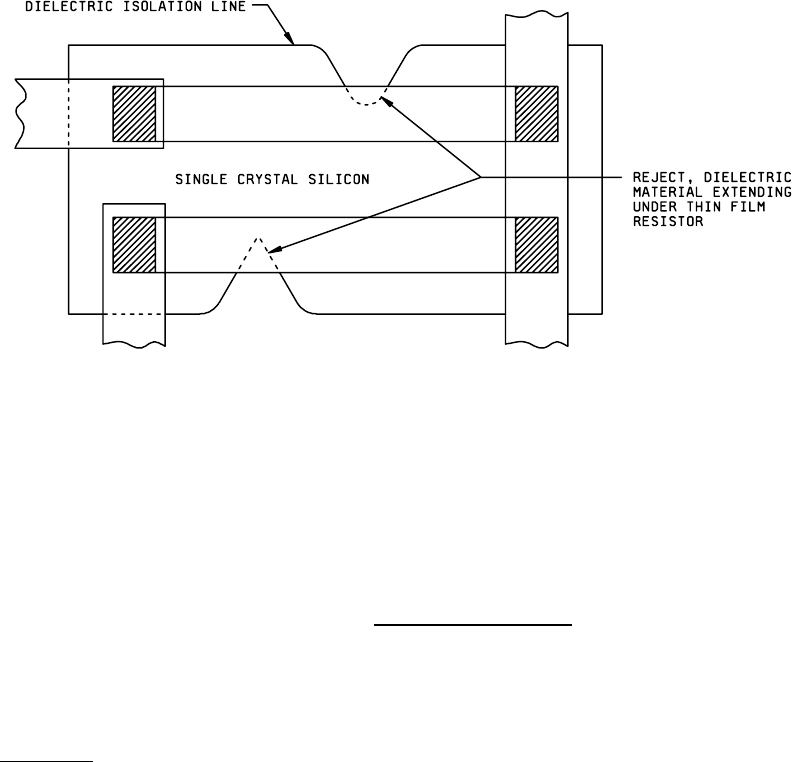
f. Any thin film resistor that crosses a substrate irregularity (e.g., dielectric isolation line, oxide/diffusion step, etc.)
(see figure 2010-26).
NOTE: This criteria does not apply to square isolated islands of single crystal silicon in the polysilicon area.
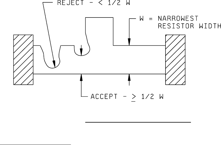
g. Any resistor width reduced to less than one half the narrowest resistor width, resulting from voids or scratches or
a combination thereof (see figure 2010-29).
NOTE: Maximum allowable current density requirements shall not be exceeded.
FIGURE 2010-29. Scratch and void criteria for untrimmed resistors
.
h. Any sharp change in color of resistor material within 0.1 mil of the resistor/connector termination.
3.1.7 Laser-trimmed thin-film resistors
. Rejection shall be based on defects found within the actively used portions of the
film resistor. No device shall be acceptable that exhibits:
a. A kerf less than 0.1 mil in width, unless by design.
NOTE: Criteria does not apply for edge trimming.
b. A kerf containing particles of detritus.