MIL- STD-883F 2004 TEST METHOD STANDARD MICROCIRCUITS.pdf - 第249页
MIL-STD-883F METHOD 2010.11 18 June 2004 39 Condition A Conditi on B Class le vel S Class lev el B h. Bonds where mor e than 25 perc ent of the bond i s loc ated on die mount ing mater ial. i. Any evidence of repair of c…
MIL-STD-883F
METHOD 2010.11
18 June 2004
38
Condition A Condition B
Class level S Class level B
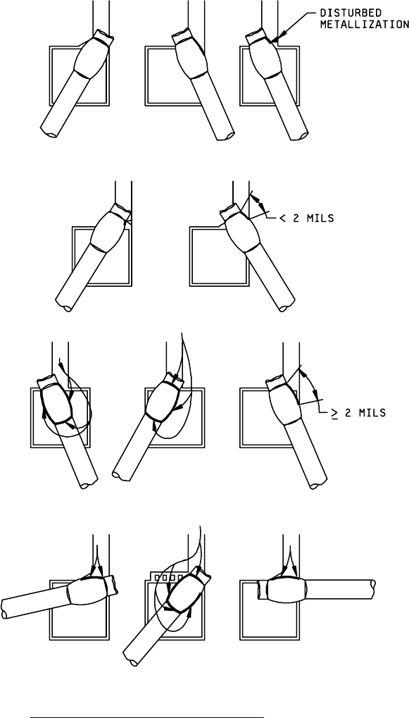
Reject: Bond (excluding tails)
placed, such that less than 2.0
mils of bond periphery (on
glassivated or unglassivated
areas) is exposed by an
undisturbed die metallization
connecting path to/from the
entering/exiting metallization
stripe.
Reject: When bond tails prevent
visibility of the connecting path
to the bond periphery and the
metallization immediately adjacent
to the bond tail is disturbed.
Accept: Bonds (excluding tails)
placed, such that there is 2.0
mils or greater of bond periphery
(on glassivated or unglassivated
areas) exposed by an undisturbed
die metallization connecting path
to/from the entering/exiting
metallization stripe.
Arrows demonstrate the connecting
path to the bond periphery.
FIGURE 2010-34. Bonds at entering/exiting metallization stripe
.

MIL-STD-883F
METHOD 2010.11
18 June 2004
39
Condition A Condition B
Class level S Class level B
h. Bonds where more than 25 percent of the bond is located on die mounting material.
i. Any evidence of repair of conductors by bridging with additional material.
j. Bonds on foreign material.
k. Intermetallic formation extending radially more than 0.1 mil completely around the periphery of that portion of the
gold bond located on metal.
3.2.1.5 Rebonding of monolithic devices
. Rebonding of monolithic microcircuits, may be done with the following
limitations. No device shall be acceptable that exhibits:
a. Rebond over exposed passivation or over metal which shows evidence of peeling. More than one rebond attempt
at any design bond location. Rebonds that touch an area of exposed oxide caused by lifted metal.
b. A bond on top of, or partially on top of, another b. Bond along side or partially on top of
bond, bond wire tail, or residual segment of wire. another bond, bond wire tail or residual
segment of wire, when the overlap width
is greater than 25 percent.
c. Rebond attempts that exceed 10 percent of the total number of bonds in the microcircuit. (e.g., for a 28 lead wire
bonded package there are 56 bonds. A bond of one end of a wire shall count as a single attempt. A replacement
of a wire bonded at both ends, counts as two rebond attempts.)
NOTE: For class level B only. Bond-offs required to
clear the bonder after an unsuccessful first bond
attempt are not considered as rebonds provided
they can be identified as bond-offs.
d. Missing or extra wires.
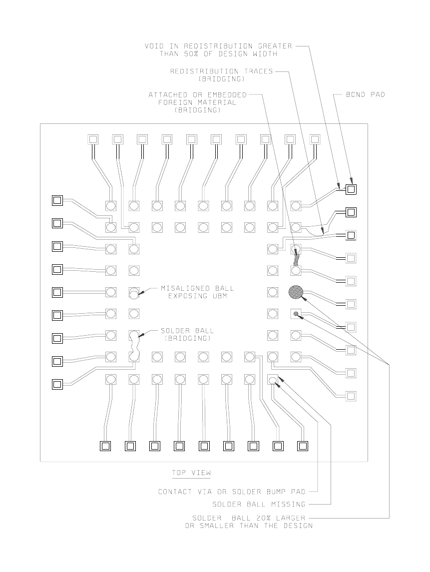
3.2.1.6 Flip chip solder bump die
. No solder bumped die shall be acceptable that exhibit any of the following
characteristics (see figure 2010-34A):
a. missing solder ball from original design position.
b. Solder ball 20% smaller, or larger than design size (nominal).
c. Solder balls bridging.
d. Any attached or embedded foreign material bridging balls, or redistribution metalization.
e. Misaligned solder ball which exposes the UBM on the contact via.
f. Voids in redistribution metalization greater than 50% of the design width.
g. Any redistribution metalization bridging.
h. Any residual unetched UBM bridging balls or redistribution metalization.
i. Mechanical damage to the ball which reduces the original height or diameter more than 20%.
j. Lifting, or peeling or the RDL or dielectric material.
Note: Minor damage to the solder ball and bump misalignment can be reworked by performing a re-flow/refresh of the
solder balls.
MIL-STD-883F
METHOD 2010.11
18 June 2004
40
Figure 2010.34A – FLIP CHIP VISUAL INSPECTION DIAGRAM