MIL- STD-883F 2004 TEST METHOD STANDARD MICROCIRCUITS.pdf - 第250页
MIL-STD-883F METHOD 2010.11 18 June 2004 40 Figure 2010.34A – FLI P CHIP VISUAL I NSPECTION DIAGRAM

MIL-STD-883F
METHOD 2010.11
18 June 2004
39
Condition A Condition B
Class level S Class level B
h. Bonds where more than 25 percent of the bond is located on die mounting material.
i. Any evidence of repair of conductors by bridging with additional material.
j. Bonds on foreign material.
k. Intermetallic formation extending radially more than 0.1 mil completely around the periphery of that portion of the
gold bond located on metal.
3.2.1.5 Rebonding of monolithic devices
. Rebonding of monolithic microcircuits, may be done with the following
limitations. No device shall be acceptable that exhibits:
a. Rebond over exposed passivation or over metal which shows evidence of peeling. More than one rebond attempt
at any design bond location. Rebonds that touch an area of exposed oxide caused by lifted metal.
b. A bond on top of, or partially on top of, another b. Bond along side or partially on top of
bond, bond wire tail, or residual segment of wire. another bond, bond wire tail or residual
segment of wire, when the overlap width
is greater than 25 percent.
c. Rebond attempts that exceed 10 percent of the total number of bonds in the microcircuit. (e.g., for a 28 lead wire
bonded package there are 56 bonds. A bond of one end of a wire shall count as a single attempt. A replacement
of a wire bonded at both ends, counts as two rebond attempts.)
NOTE: For class level B only. Bond-offs required to
clear the bonder after an unsuccessful first bond
attempt are not considered as rebonds provided
they can be identified as bond-offs.
d. Missing or extra wires.
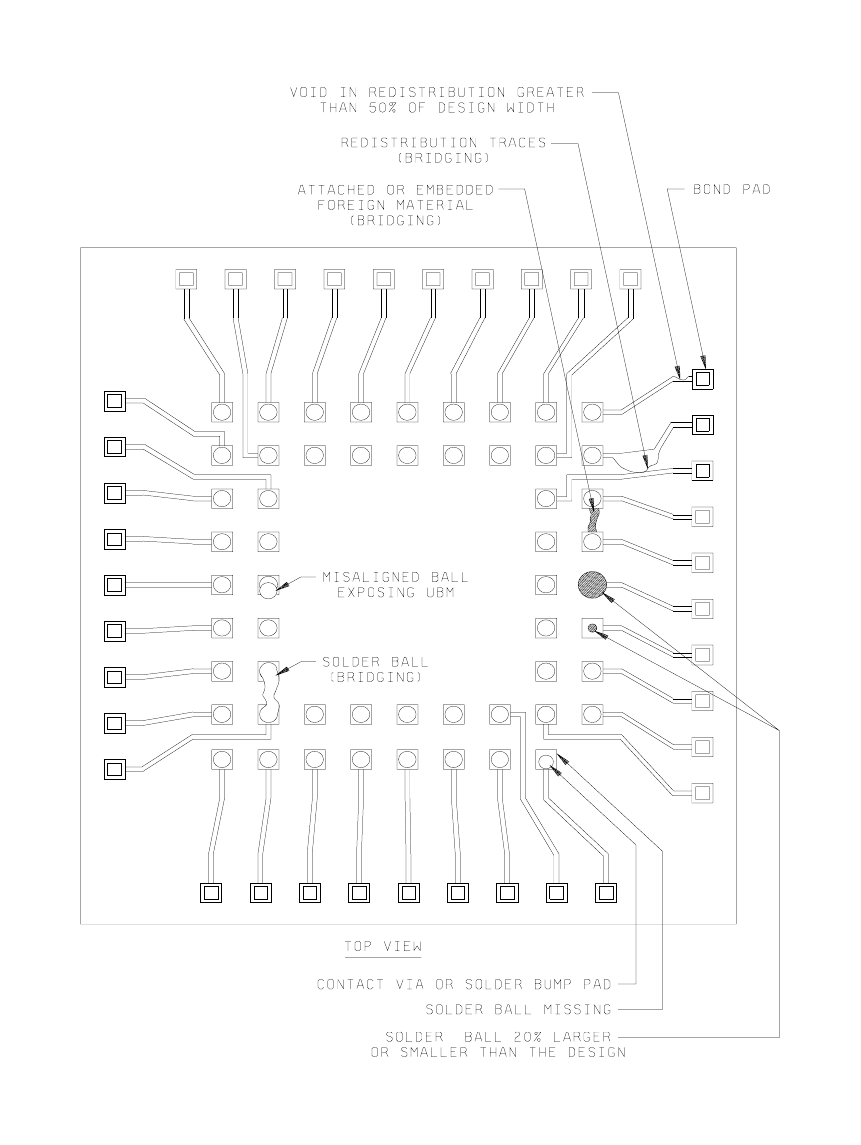
3.2.1.6 Flip chip solder bump die
. No solder bumped die shall be acceptable that exhibit any of the following
characteristics (see figure 2010-34A):
a. missing solder ball from original design position.
b. Solder ball 20% smaller, or larger than design size (nominal).
c. Solder balls bridging.
d. Any attached or embedded foreign material bridging balls, or redistribution metalization.
e. Misaligned solder ball which exposes the UBM on the contact via.
f. Voids in redistribution metalization greater than 50% of the design width.
g. Any redistribution metalization bridging.
h. Any residual unetched UBM bridging balls or redistribution metalization.
i. Mechanical damage to the ball which reduces the original height or diameter more than 20%.
j. Lifting, or peeling or the RDL or dielectric material.
Note: Minor damage to the solder ball and bump misalignment can be reworked by performing a re-flow/refresh of the
solder balls.
MIL-STD-883F
METHOD 2010.11
18 June 2004
40
Figure 2010.34A – FLIP CHIP VISUAL INSPECTION DIAGRAM

MIL-STD-883F
METHOD 2010.11
18 June 2004
41
Condition A Condition B
Class level S Class level B
3.2.2 Internal wires
. During inspection for the requirements of 3.2.2, each device shall be viewed at any angle necessary
to determine full compliance to this specification, without damaging the device. No device shall be acceptable that exhibits:
a. Any wire with a separation of less than two wire a. Any wire with a separation of less than one
diameters to unglassivated operating metal,other wire diameter to unglassivated operating
bonds, another wire (common wiresexcluded),other metal, other bonds, another wire (common
package post, unglassivated die area (except for wires excluded), other package post,
wires or pads which are at the die or substrate unglassivated die area (except for wires or
potential), or any portion of the package pads which are at the die or substrate
including the plane of the lid to be attached. potential), or any conductive portion of the
package or the plane of the lid to be
attached.
NOTE: For condition A only. Within a 5.0 mil NOTE: For condition B only. Within a
radial distance from the perimeter of the bond 10.0 mil radial distance from the perimeter
on the die the separation shall be 1.0 mil of the bond on the die a line of separation
minimum. must be visible.
NOTE: For SOS devices, exclude the unglassivated insulator areas.
b. Nicks, bends, cuts, crimps, scoring, or neckdown in any wire that reduces the wire diameter by more than 25
percent.
c. Tearing at the junction of the wire and bond.
d. Any wire making a straight line run from a die bonding pad to a package post that has no arc.