MIL- STD-883F 2004 TEST METHOD STANDARD MICROCIRCUITS.pdf - 第263页
MIL-STD-883F METHOD 2011.7 22 March 1989 3 b. For external bonds connec ting devi ce to wi ring boar d or subs trat e: (b-1) Lead or t erminal break at deformat ion point (weld af fect ed region) . (b-2) Lead or t ermina…

MIL-STD-883F
METHOD 2011.7
22 March 1989
2
3.1.3 Test condition D - Wire pull (double bond). This procedure is identical to that of test condition C, except that the
pull is applied by inserting a hook under the lead wire (attached to die, substrate or header or both ends) with the device
clamped and the pulling force applied approximately in the center of the wire in a direction approximately normal to the
die or substrate surface or approximately normal to a straight line between the bonds. When a failure occurs, the force
causing the failure and the failure category shall be recorded. The minimum bond strength shall be taken from table I.
Figure 2011-1 may be used for wire diameters not specified in table I. For wire diameter or equivalent cross section
>0.005 inch, where a hook will not fit under the wire, a suitable clamp can be used in lieu of a hook.
3.1.4 Test condition F - Bond shear (flip chip)
. This test is normally employed for internal bonds between a
semiconductor die and a substrate to which it is attached in a face-bonded configuration. It may also be used to test the
bonds between a substrate and an intermediate carrier or secondary substrate to which the die is mounted. A suitable
tool or wedge shall be brought in contact with the die (or carrier) at a point just above the primary substrate and a force
applied perpendicular to one edge of the die (or carrier) and parallel to the primary substrate, to cause bond failure by
shear. When a failure occurs, the force at the time of failure, and the failure category shall be recorded.
3.1.5 Test condition G - Push-off test (beam lead)
. This test is normally employed for process control and is used on
a sample of semiconductor die bonded to a specially prepared substrate. Therefore, it cannot be used for random
sampling of production or inspection lots. A metallized substrate containing a hole shall be employed. The hole
appropriately centered, shall be sufficiently large to provide clearance for a push tool, but not large enough to interfere
with the bonding areas. The push tool shall be sufficiently large to minimize device cracking during testing, but not large
enough to contact the beam leads in the anchor bond area. Proceed with push-off tests as follows: The substrate shall
be rigidly held and the push tool inserted through the hole. The contact of the push tool to the silicon device shall be
made without appreciable impact (less than 0.01 inch/minute (0.254 mm/minute ) and forced against the underside of
the bonded device at a constant rate. When failure occurs, the force at the time of failure, and the failure category shall
be recorded.
3.1.6 Test condition H - Pull-off test (beam lead)
. This test is normally employed on a sample basis on beam lead
devices which have been bonded down on a ceramic or other suitable substrate. The calibrated pull-off apparatus (see
2) shall include a pull-off rod (for instance, a current loop of nichrome or Kovar wire) to make connection with a hard
setting adhesive material (for instance, heat sensitive polyvinyl acetate resin glue) on the back (top side) of the beam
lead die. The substrate shall be rigidly installed in the pull-off fixture and the pull-off rod shall make firm mechanical
connection to the adhesive material. The device shall be pulled within 5 degrees of the normal to at least the calculated
force (see 3.2), or until the die is at 2.54 mm (0.10 inch) above the substrate. When a failure occurs, the force at the
time of failure, the calculated force limit, and the failure category shall be recorded.
3.2 Failure criteria
. Any bond pull which results in separation under an applied stress less than that indicated in
table I as the required minimum bond strength for the indicated test condition, composition, and construction shall
constitute a failure.
3.2.1 Failure category
. Failure categories are as follows: When specified, the stress required to achieve separation
and the category of separation or failure shall be recorded.
a. For internal wire bonds:
(a-1) Wire break at neckdown point (reduction of cross section due to bonding process).
(a-2) Wire break at point other than neckdown.
(a-3) Failure in bond (interface between wire and metallization) at die.
(a-4) Failure in bond (interface between wire and metallization) at substrate, package post, or other than die.
(a-5) Lifted metallization from die.
(a-6) Lifted metallization from substrate or package post.
(a-7) Fracture of die.
(a-8) Fracture of substrate.
MIL-STD-883F
METHOD 2011.7
22 March 1989
3
b. For external bonds connecting device to wiring board or substrate:
(b-1) Lead or terminal break at deformation point (weld affected region).
(b-2) Lead or terminal break at point not affected by bonding process.
(b-3) Failure in bond interface (in solder or at point of weld interface between lead or terminal and the board or
substrate conductor to which the bond was made).
(b-4) Conductor lifted from board or substrate.
(b-5) Fracture within board or substrate.
c. For flip-chip configurations:
(c-1) Failure in the bond material or pedestal, if applicable.
(c-2) Fracture of die (or carrier) or substrate (removal of portion of die or substrate immediately under the bond).
(c-3) Lifted metallization (separation of metallization or bonding pedestal from die (or carrier) or substrate.
d. For beam lead devices:
(d-1) Silicon broken.
(d-2) Beam lifting on silicon.
(d-3) Beam broken at bond.
(d-4) Beam broken at edge of silicon.
(d-5) Beam broken between bond and edge of silicon.
(d-6) Bond lifted.
(d-7) Lifted metallization (separation of metallization) from die, separation of bonding pad.
(d-8) Lifted metallization.
NOTE: RF/microwave hybrids that require extremely flat loops which may cause erroneous wire pull data may use the
following formula to determine the proper wire pull value.
V
1
= V
2
sin Θ
Where: V
1
= New value to pull test.
V
2
= Table I value for size wire tested.
Θ = Greatest calculated wire loop angle (figure 2011-2).
Also, RF/microwave hybrids that contain wires that cannot be accessed with a pull hook must be duplicated on a test
coupon in such a way to allow hook access for purposes of pull testing. These wires are to be bonded at the same time
the production hybrids are bonded using the same setup, operator, and schedule. The test coupon wires are to be pull
tested in lieu of the tuning or inaccessible wires on the production hybrid. Failures on the test coupon shall be
considered as failures to production units and appropriate action is to be taken in accordance with the applicable
specification (figure 2011-3).
MIL-STD-883F
METHOD 2011.7
22 March 1989
4
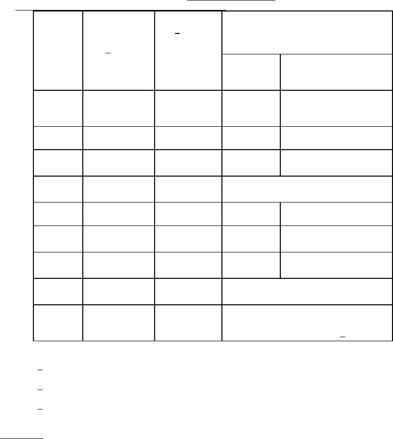
TABLE I. Minimum bond strength.
Test
condition
Wire
composition
and diameter
1
/
Construction
2
/
Minimum bond strength (grams force)
Pre seal Post seal and any other
processing and screening
when applicable
A --- --- Given in
applicable
document
Given in applicable
document
C or D AL 0.0007 in
AU 0.0007 in
Wire 1.5
2.0
1.0
1.5
C or D AL 0.0010 in
AU 0.0010 in
Wire 2.5
3.0
1.5
2.5
C or D AL 0.00125 in
AU 0.00125 in
Wire Same bond strength limits
as the 0.0013 in wire
C or D AL 0.0013 in
AU 0.0013 in
Wire 3.0
4.0
2.0
3.0
C or D AL 0.0015 in
AU 0.0015 in
Wire 4.0
5.0
2.5
4.0
C or D AL 0.0030 in
AU 0.0030 in
Wire 12.0
15.0
8.0
12.0
F Any Flip-clip 5 grams-force x
number of bonds (bumps)
G or H Any Beam lead 30 grams force in accordance with
linear millimeter of nominal undeformed
(before bonding) beam width. 3
/
1
/ For wire diameters not specified, use the curve of figure 2011-1 to determine the bond
pull limit.
2
/ For ribbon wire, use the equivalent round wire diameter which gives the same
cross-sectional area as the ribbon wire being tested.
3
/ For condition G or H, the bond strength shall be determined by dividing the breaking
force by the total of the nominal beam widths before bonding.
4. SUMMARY
. The following details shall be specified in the applicable acquisition document:
a. Test condition letter (see 3).
b. Minimum bond strength if other than specified in 3.2 or details of required strength distributions if applicable.
c. Sample size number and accept number or number and selection of bond pulls to be tested on each device, and
number of devices, if other than 4.
d. For test condition A, angle of bond peel if other than 90°, and bond strength limit (see 3.2).
e. Requirement for reporting of separation forces and failure categories, when applicable (see 3.2.1).