MIL- STD-883F 2004 TEST METHOD STANDARD MICROCIRCUITS.pdf - 第276页
MIL-STD-883F METHOD 2012.7 1 June 1993 10 3.11 Examination and ac ceptanc e cr iter ia for hybr id devic es . 3.11.1 Devi ce cons truc tion . Acc eptable devi ces s hall be of the spec ifi ed design and c onst ruct ion w…
MIL-STD-883F
METHOD 2012.7
1 June 1993
9
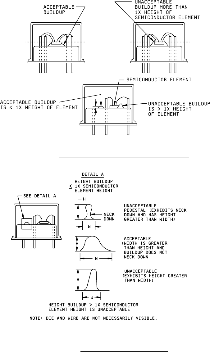
FIGURE 2012-2. Acceptable and unacceptable bonding material build-up
.
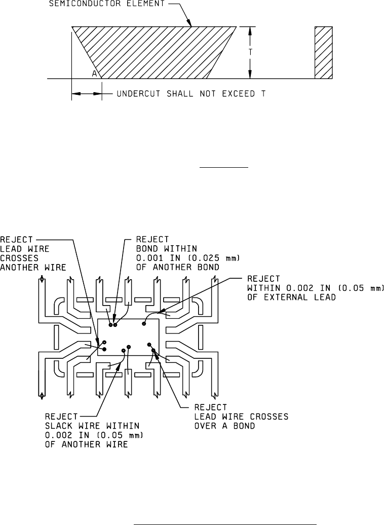
FIGURE 2012-3. Extraneous bonding material build-up
.

MIL-STD-883F
METHOD 2012.7
1 June 1993
10
3.11 Examination and acceptance criteria for hybrid devices.
3.11.1 Device construction
. Acceptable devices shall be of the specified design and construction with regard to the
characteristics discernible through radiographic examination. Devices that deviate significantly from the specified
construction shall be rejected.
3.11.2 Individual device defects
. The individual device examination shall include, but not be limited to, extraneous
matter, location and orientation of elements, cracks in the substrate that exceed 0.127 mm (0.005 inch) in length or point
toward active metallization, adhesive build-up, solder splashes, placement of wires, voids in the lid seal (this may not
apply to power hybrid devices), and improper wetting between the substrate(s) and the package. Any device for which
the radiograph reveals any of the following defects shall be rejected:
3.11.2.1 Presence of extraneous matter (foreign particles)
.
a. Unattached foreign material greater than 0.025 mm (0.001 inch), or of any lesser size which is sufficient to bridge
metallization or nonconnected conducting elements, that appears to be on the surface of the die, component,
substrate, or within the package.
b. Attached foreign material that bridges metallization paths, package leads, lead to package metallization, functional
circuit elements, junctions, or any combination thereof.
NOTE: Attached or unattached material may be verified by comparing two identical views with a mild mechanical
shock, such as PIND test, between the two views.
c. Wire tails or extra wires which make contact with any metallization not connected to the wire, or which exceed four
wire diameters in length at the substrate pad or package post, or two wire diameters at the top of a die or
component.
d. Any evidence of solder, alloy, or conductive adhesive that appears to bridge noncommon metallization (i.e., wire(s),
bonding post, active metallization or any combination thereof) not intended by design.
e. Gold flaking on the bonding post or anywhere inside the case.
3.11.2.2 Unacceptable construction
.
a. voids in substrate or component attachment medium.
(1) Contact area voids in excess of one-half of the total contact area.
(2) A single void which traverses either the length or width of the substrate or semiconductor element
and whose area exceeds 10 percent of the total intended contact area.
NOTE: To obtain, and/or verify substrate attachment the use of a thermal resistance analyzer, which
measures the thermal characteristics (heat dissipation), is strongly recommended.
b. Wires present, other than those connecting specific areas as per the drawing, except wires designated as tuning
devices on the bonding diagram, and except where bond-offs are allowed.
c. Improper component placement.
d. Cracks, splits, or chips in the component or substrate which enter the active circuit area.
MIL-STD-883F
METHOD 2012.7
1 June 1993
11
NOTE: Angle A shall be greater than 45°.
FIGURE 2012-4 Undercutting
.
FIGURE 2012-5. Clearance in dual-in-line or flat pack type device
.