MIL- STD-883F 2004 TEST METHOD STANDARD MICROCIRCUITS.pdf - 第294页
MIL-STD-883F METHOD 2017.8 18 June 2004 4 h. Foreign mat erial c ontrol . The manufac turer shall perfor m an audit on a week ly basi s for the pres ence of f oreign materi al on the die s urfac e, or within t he package…

MIL-STD-883F
METHOD 2017.8
18 June 2004
3
(15) Insulating layer
is a dielectric layer used to isolate single or multilevel conductive and resistive material or to
protect top level conductive resistive material.
(16) Intermetallics (Purple Plague)
is one of several gold-aluminum compounds formed when bonding gold to
aluminum and activated by re-exposure to moisture and high temperature (>340°C). Purple plague is purplish
in color and is very brittle, potentially leading to time-based failure of the bonds. Its growth is highly enhanced
by the presence of silicon to form ternary compounds.
(17) Mechanical strength tests
are tests, such as Mechanical Shock or Constant Acceleration, which demonstrate
adequate attachment process and materials.
(18) Non-monometallic compound bond
consists of two lead bonds, made of dissimilar metals, which are stacked
one on top of the other (i.e., the interface between the two lead bonds are made up of dissimilar metals such as
an aluminum lead bond stacked on top of a gold lead bond or vice-versa.
(19) Operating metallization (conductors)
is all metal or any other material used for interconnections except
metallized scribe lines, test patterns, unconnected functional circuit elements, unused bonding pads and
identification markings.
(20) Original design separation
is the separation dimension or distance that is intended by design.
(21) Original width
is the width dimension or distance that is intended by design (i.e., original metal width, original
diffusion width, original beam width, etc.).
(22) Passivation
is the silicon oxide, nitride, or other insulating material that is grown or deposited directly on the die
prior to the deposition of the final metal layers.
(23) String
is a filamentary run-out or whisker of polymer material.
(24) Substrate
is the supporting structural material into and/or upon which the passivation, metallization, and circuit
elements are placed.
(25) Tuning
is the adjustment of signals from an RF/Microwave circuit by altering lines or pads; adding, deleting or
manipulating wires/ribbons; and/or changing resistance, inductance or capacitance values to meet specific
electrical specifications.
(26) Through hole metallization
is the metallization that electrically connects the metallization on the top surface of
the substrate to the opposite surface of the substrate.
(27) Unused component or unused deposited element
is one not connected to a circuit or connected to a circuit
path at one and only one point. A connection may be made by design or by visual anomaly.
(28) Void
is any region in the material (interconnects, bonding sites, etc.) where underlying material is visible that is
not caused by a scratch.
(29) Visible line
is defined as 0.5 mil at 60X magnification.
g. Interpretations
. References herein to "that exhibits" shall be considered satisfied when the visual image or visual
appearance of the device under examination indicates a specific condition is present and shall not require
confirmation by any other method of testing. When other methods of test are to be used to confirm that a reject
condition does not exist, they shall be approved by the acquiring activity.

MIL-STD-883F
METHOD 2017.8
18 June 2004
4
h. Foreign material control
. The manufacturer shall perform an audit on a weekly basis for the presence of foreign
material on the die surface, or within the package. This audit may be satisfied during routine internal visual
inspection. If the presence of any type of foreign material/contamination is discovered, the manufacturer shall
perform the necessary analysis on a sample of suspect devices to determine the nature of the foreign material.
The manufacturer shall then document the results of his investigation and corrective actions to eliminate the
foreign material and shall make this information available to the Government QAR, the acquiring activity, or the
qualifying activity, as required. Corrective action responses shall be obtained within a maximum of ten (10)
working days of discovery. The intent of this procedure is to require investigation and resolution of foreign
material/contamination problems which do not have effective screening or detection methodology, but that could
cause degradation and eventual failure of the device function. Repetitive findings without obvious improvements
require escalation to Director of Manufacturing and Director of Quality Assurance, or their equivalents, to continue
processing.
3.1 Examination
. Internal visual examination as required in 3.1.1 through 3.1.9 shall be conducted on each SAW,
hybrid/multichip microcircuit, or microwave hybrid microcircuit. The magnifications required for each inspection shall be
those identified in the particular test method used (i.e., 2010, 2017, or 2032 of MIL-STD-883 and 2072, 2073 of
MIL-STD-750).
3.1.1 Active and passive elements
. All integrated circuit elements shall be examined in accordance with MIL-STD-883,
method 2010.
Class H
Class K
(Class level B Monolithic) (Class level S Monolithic)
Method 2010; Para. 3.1.1: Metallization defects.
Method 2010; Para. 3.1.2: Diffusion and passivation layer(s) faults.
Method 2010; Para. 3.1.3: Scribing and die defects.
Method 2010; Para. 3.2.5: Foreign material.
Method 2010; Para. 3.1.4: Glassivation defects.
Method 2010; Para 3.1.6: Film resistors defects.
Method 2010; Para. 3.1.7: Laser trimmed film resistor defects.
Transistor and semiconductor diode elements shall be examined in accordance with MIL-STD-883, method 2010
(paragraphs referenced above) or the identified paragraphs of MIL-STD-750, methods 2072 and 2073 as indicated below.
Passive elements (including substrates) shall be examined in accordance with MIL-STD-883, method 2032.
Visual MIL-STD-750 MIL-STD-883
Inspection
Method 2072 Method 2073 Method 2010
Die metallization 4.1.1 4.1.3, 4.1.5 3.1.1
defects
Diffusion and 4.1.2 4.1.2 3.1.2
passivation
layer(s)
Scribing and die 4.1.3 4.1.1, 4.1.4 3.1.3
defects
MIL-STD-883F
METHOD 2017.8
18 June 2004
5
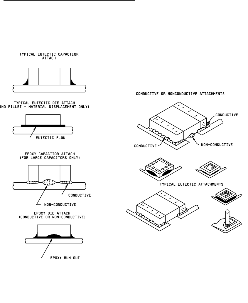
3.1.2 Element attachment (assembly), "magnification 10X to 60X"
. Figures 2017-1 and 2017-2 are example visual
representations of attachment media types.
NOTE: Rejection criteria are not to be derived from these examples but rather from the specific criteria paragraphs that
follow.
FIGURE 2017-1. Element attachments
. FIGURE 2017-2. Element attachments.