MIL- STD-883F 2004 TEST METHOD STANDARD MICROCIRCUITS.pdf - 第295页
MIL-STD-883F METHOD 2017.8 18 June 2004 5 3.1. 2 Element att achment ( assembl y), "magni ficat ion 10X to 60X" . Figur es 2017-1 and 2017- 2 are example vis ual repres entati ons of at tachment media types . N…

MIL-STD-883F
METHOD 2017.8
18 June 2004
4
h. Foreign material control
. The manufacturer shall perform an audit on a weekly basis for the presence of foreign
material on the die surface, or within the package. This audit may be satisfied during routine internal visual
inspection. If the presence of any type of foreign material/contamination is discovered, the manufacturer shall
perform the necessary analysis on a sample of suspect devices to determine the nature of the foreign material.
The manufacturer shall then document the results of his investigation and corrective actions to eliminate the
foreign material and shall make this information available to the Government QAR, the acquiring activity, or the
qualifying activity, as required. Corrective action responses shall be obtained within a maximum of ten (10)
working days of discovery. The intent of this procedure is to require investigation and resolution of foreign
material/contamination problems which do not have effective screening or detection methodology, but that could
cause degradation and eventual failure of the device function. Repetitive findings without obvious improvements
require escalation to Director of Manufacturing and Director of Quality Assurance, or their equivalents, to continue
processing.
3.1 Examination
. Internal visual examination as required in 3.1.1 through 3.1.9 shall be conducted on each SAW,
hybrid/multichip microcircuit, or microwave hybrid microcircuit. The magnifications required for each inspection shall be
those identified in the particular test method used (i.e., 2010, 2017, or 2032 of MIL-STD-883 and 2072, 2073 of
MIL-STD-750).
3.1.1 Active and passive elements
. All integrated circuit elements shall be examined in accordance with MIL-STD-883,
method 2010.
Class H
Class K
(Class level B Monolithic) (Class level S Monolithic)
Method 2010; Para. 3.1.1: Metallization defects.
Method 2010; Para. 3.1.2: Diffusion and passivation layer(s) faults.
Method 2010; Para. 3.1.3: Scribing and die defects.
Method 2010; Para. 3.2.5: Foreign material.
Method 2010; Para. 3.1.4: Glassivation defects.
Method 2010; Para 3.1.6: Film resistors defects.
Method 2010; Para. 3.1.7: Laser trimmed film resistor defects.
Transistor and semiconductor diode elements shall be examined in accordance with MIL-STD-883, method 2010
(paragraphs referenced above) or the identified paragraphs of MIL-STD-750, methods 2072 and 2073 as indicated below.
Passive elements (including substrates) shall be examined in accordance with MIL-STD-883, method 2032.
Visual MIL-STD-750 MIL-STD-883
Inspection
Method 2072 Method 2073 Method 2010
Die metallization 4.1.1 4.1.3, 4.1.5 3.1.1
defects
Diffusion and 4.1.2 4.1.2 3.1.2
passivation
layer(s)
Scribing and die 4.1.3 4.1.1, 4.1.4 3.1.3
defects
MIL-STD-883F
METHOD 2017.8
18 June 2004
5
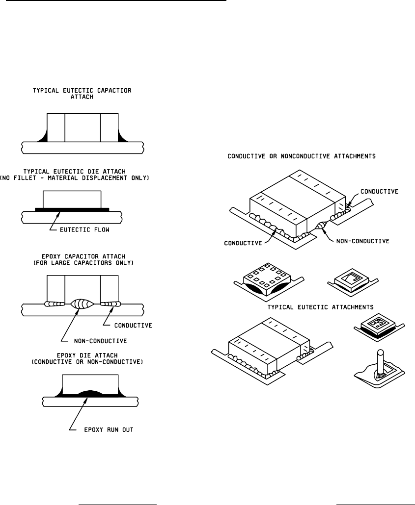
3.1.2 Element attachment (assembly), "magnification 10X to 60X"
. Figures 2017-1 and 2017-2 are example visual
representations of attachment media types.
NOTE: Rejection criteria are not to be derived from these examples but rather from the specific criteria paragraphs that
follow.
FIGURE 2017-1. Element attachments
. FIGURE 2017-2. Element attachments.

MIL-STD-883F
METHOD 2017.8
18 June 2004
6
Class H
Class K
Note: Mechanical strength or Dielectric attachment may be
Radiography may be used to assessed through Mechanical Strength
verify attachment in lieu of Testing. For conductive attachment,
visual criteria. the Qualifying Activity may approve
alternate methods for verifying
attachment integrity.
No device shall be acceptable that exhibits:
a. For non-end terminated elements, attachment media not visible around at least 50 percent of the perimeter unless
it is continuous on two full nonadjacent sides of the element.
NOTE: The criteria of paragraph 3.1.2.a shall not apply when attachment material is applied directly to more than 50
percent of the element attach area by use of a method such as preforms or printing.
b. End terminated elements that do End terminated elements that do not
not have conductive attachment have conductive attachment media
media visible around at least visible around at least 75 percent
50 percent of the visible of the visible bonding pad perimeter
bonding pad perimeter on each on each end termination. For
end termination. For dielectric attachment of end
dielectric attachment of end terminated elements (i.e., where
terminated elements (i.e., the body of the element between the
where the body of the element end terminations is attached), the
between the end terminations is criteria of (a) above applies.
attached), the criteria of (a)
above applies.
c. Glass substrates or transparent die, when viewed from the bottom, which exhibit attach area less than 50 percent.
NOTE: This criterion may be employed in lieu of 3.1.2.a.
d. Flaking of the attachment media material.
e. Balling of the solder or alloy material that does not exhibit a fillet. (see Figure 2017-3)