MIL- STD-883F 2004 TEST METHOD STANDARD MICROCIRCUITS.pdf - 第302页
MIL-STD-883F METHOD 2017.8 18 June 2004 12 Class H Class K a. One bond used to s ecure t wo common wir es. ( see Figur e 2017-5) FIGURE 2017-5. One bond used to s ecure two c ommon wires . b. More than one bond on t op o…
MIL-STD-883F
METHOD 2017.8
18 June 2004
11
Class H Class K
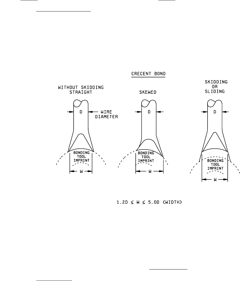
3.1.5.3 Tailless bonds (crescent)
. No device shall be acceptable that exhibits:
a. Tailless bonds that are less than 1.2 times or greater than 5.0 times the wire diameter in width. (see Figure
2017-4b).
b. A tailless bond of a gold wire bonded on the aluminum pads of a die.
FIGURE 2017-4b. Bond Dimensions
.
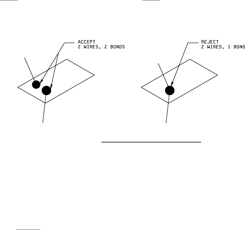
3.1.5.4 Compound bond
. No device shall be acceptable that exhibits the following:
NOTE: Broken or lifted bonds as a result of electrical troubleshooting or tuning shall be considered rework and shall not
apply to the 10 percent repair limitation.
*
MIL-STD-883F
METHOD 2017.8
18 June 2004
12
Class H Class K
a. One bond used to secure two common wires. (see Figure 2017-5)
FIGURE 2017-5. One bond used to secure two common wires
.
b. More than one bond on top of original bond.
NOTE: When required by design and based on a justifiable technical need, and with the approval of the qualifying
or acquiring activity, additional compound bonds may be allowed in addition to the limitations of a and b
above. Demonstration of acceptable N+1 bond stacks (N = maximum number of compound bonds
allowable by the manufactures process) and establishment of necessary process controls shall be
required for approval.
c. Compound bond where the contact area of the second bond with the original bond is less than 75 percent of the
bottom bond.
d. Non-monometallic compound bond (i.e., between dissimilar metals, excluding the bond pad metallization).
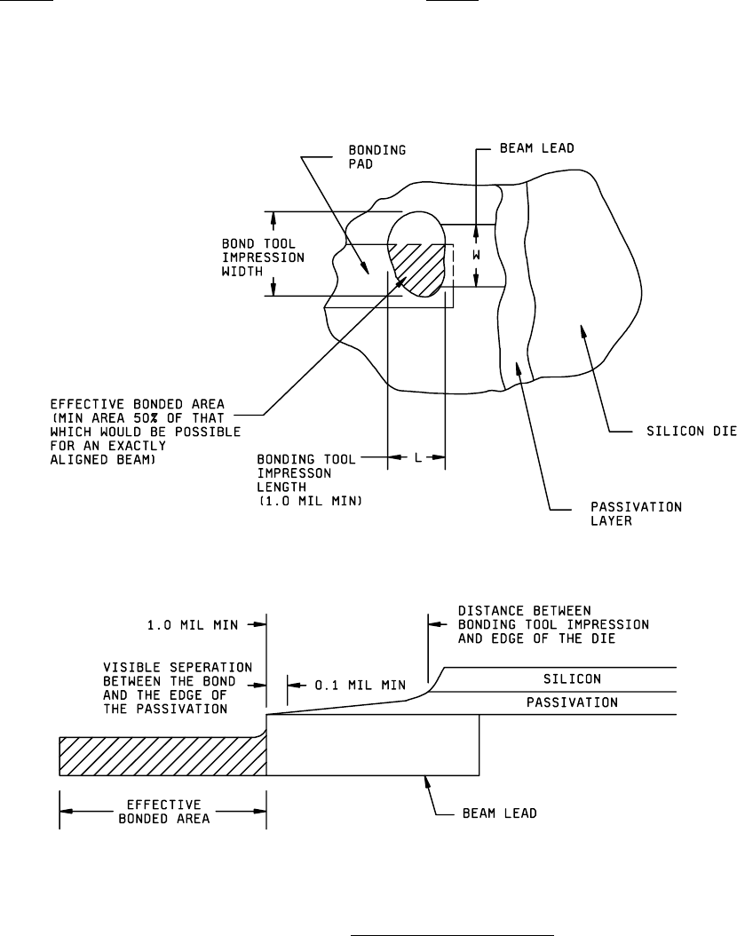
3.1.5.5 Beam lead
. This inspection and criteria shall apply to the completed bond area made using direct tool contact.
No device shall be acceptable that exhibits:
a. Bonds which do not exhibit 100 percent bond/weld impression(s) across the width of the beam lead.
NOTE: Gaps between bonds/welds on the beam lead caused by the natural footprint of a bond/weld tip (i.e., split
tip, etc.), are acceptable provided the total of all gaps does not exceed 25 percent of the beam lead width.
b. Complete or partial beam separation from the die.
c. Bonds on the substrate where the tool impression is not visible on the beam.
d. Beam lead width increased by greater than 60 percent of the original beam width.
MIL-STD-883F
METHOD 2017.8
18 June 2004
13
Class H Class K
e. Bonds where the tool impression length is less than 1.0 mil (see Figure 2017-6)
FIGURE 2017-6. Beam Lead Area and Location
.