MIL- STD-883F 2004 TEST METHOD STANDARD MICROCIRCUITS.pdf - 第308页
MIL-STD-883F METHOD 2017.8 18 June 2004 18 Class H Class K 3.1. 7 Screw t abs and thr ough hole mounti ng, magnifi cati on 3X to 10X . No devic e shall be accept able that exhibits : a. Mis aligned tabs. b. Miss ing or b…

MIL-STD-883F
METHOD 2017.8
18 June 2004
17
Class H Class K
k. Wedge, crescent or ball bonds at the point where metallization exits from the bonding pad that do not exhibit a line
of undisturbed metal visible between the periphery of the bond and at least one side of the entering metallization
stripe.
NOTE: Criteria of 3.1.5.8 (k) can be excluded when the entering conductor is >2 mils in width and the bond pad dimension
on the entering conductor side is >3.5 mils.
NOTE: For Class H only, the requirements for a visual line of metal can be satisfied when an acceptable wire tail obscures
the area of concern, provided the following condition exists. Bond is located more than 0.1 mil from the intersecting line of
the entering metallization stripe and the bonding pad and there is no visual evidence of disturbed pad metallization at the
bond and wire tail interface.
NOTE: Criteria 3.1.5.8 (k) is not applicable to interdigitated (Lange) couplers or when the interface between a
thermosonic/ultrasonic (i.e., non-thermocompression) bond and underlying metal is monometallic.
l. Polymeric adhesive which may be material or residue as evidenced by discoloration within 5.0 mils of the outer
periphery of a wire bond.
m. Tearing at the junction of the wire and bond. The junction is the line of deformation of the wire at the bonding site.
3.1.6 Internal leads (e.g., wires, ribbons, beams, wireloops, ribbon loops, beams, etc.), "magnification 10X to 60X"
. No
device shall be acceptable that exhibits:
a. Within the first 5.0 mils of wire from the die surface for ball bonds, or 10.0 mils for wedge bonds, any wire that
comes closer than 1.0 mil to any non-common conductive surface (e.g., unglassivated operating metallization,
unpassivated edge of conductive die).
NOTE: Insulated wires and electrically common wires are excluded from this criteria.
b. After the first 5.0 mils of wire from the die surface for ball bond(s), or 10 mils for wedge bonds, any wire that comes
closer than two wire diameters to any non-common, uninsulated conductive surface (e.g., unglassivated operating
metallization, unpassivated edge of conductive die).
NOTE: Insulated wires and electrically common wires are excluded from this criteria.
c. Nicks, cuts, crimps, scoring, sharp bends, or neckdown in any lead that reduces the lead diameter/width by more
than 25 percent.
d. Missing or extra lead(s) not in conformance with bonding diagram.
NOTE: Leads designated for tuning on the bonding diagram are excluded.
e. Any lead making a straight line run from bond to bond that has no arc, unless specifically allowed by the bonding
diagram.
f. Wire(s) crossing wire(s) with a separation of less than 2 lead widths. Common or insulated conductors and
insulated wires are excluded.
g. Complete or partial separation of the lead from the body of the element.
h. Excessive loop height such that the wire would contact the lid when it is installed.
*
MIL-STD-883F
METHOD 2017.8
18 June 2004
18
Class H Class K
3.1.7 Screw tabs and through hole mounting, magnification 3X to 10X
. No device shall be acceptable that exhibits:
a. Misaligned tabs.
b. Missing or broken tabs.
c. Cracks emanating from mounting holes.
d. Loose substrates.
e. Missing or loose screws.
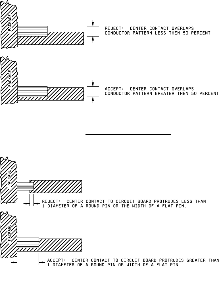
3.1.8 Connector and feedthrough center contact soldering, magnification 10X to 30X
. No device shall be acceptable that
exhibits:
a. Less than 50 percent of center contact overlaps onto metallized pattern (see Figure 2017-9).
b. Center contact to substrate protrudes over onto circuit less than 1 diameter of a round pin or the width of a flat pin
(see Figure 2017-10).
c. Voids in solder (see Figure 2017-11a).
d. Cracked solder joint (see Figure 2017-11b).
e. Poor adhesion of solder to center contact or substrate (see Figure 2017-11b).
f. Insufficient or excess solder (see Figures 2017-11c through 2017-11e).
g. Less than full coverage of solder along the length of the center contact and the metallization.
MIL-STD-883F
METHOD 2017.8
18 June 2004
19
FIGURE 2017-9 Center contact orientations to substrate.
FIGURE 2017-10. Center Contact overlap to substrate
.