MIL- STD-883F 2004 TEST METHOD STANDARD MICROCIRCUITS.pdf - 第315页
MIL-STD-883F METHOD 2018.4 18 June 2004 3 Referenc e to die or dice wi thin thi s tes t method i mplies the evaluat ion of a c omplete f uncti on or devic e. W hen appr oved by the quali fying act ivit y, thi s requi rem…

MIL-STD-883F
METHOD 2018.4
18 June 2004
2
1.1.11 Nondestructive SEM. The use of specific equipment parameters and techniques that result in negligible radiation
damage, contamination, or both of the inspected semiconductor structure (see 3.10 and 3.11).
1.1.12 Passivation
. The silicon oxide, nitride or other insulating material that is grown or deposited on the die prior to
metallization.
1.1.13 Passivation steps
. The vertical or sloped surface resulting from topographical variations of the wafer surface (e.g.,
contact windows, diffusion cuts, vias, etc.).
1.1.14 Via
. The opening in the insulating layer to provide a means for deposition of metal to interconnect layers of metal.
1.1.15 Wafer lot
. A wafer lot consists of microcircuit wafers formed into a lot at the start of wafer fabrication for
homogeneous processing as a group and assigned a unique identifier or code to provide traceability and maintain lot
integrity throughout the fabrication process.
2. APPARATUS
. The apparatus for this inspection shall be a scanning electron microscope (SEM) having resolution of
250Å or less as measured on the photograph at use conditions and a variable magnification of 1,000X to 20,000X or greater.
The apparatus shall be such that the specimen can be tilted to a viewing angle (see figure 2018-3) between 0° and 85°, and
can be rotated through 360°.
2.1 Calibration
. The magnification shall be within ±10 percent of the nominal value when compared with National Institute
of Standards and Technology standard 484 or an equivalent at the magnification(s) used for inspection. The resolution shall
be 250Å or less as verified with National Institute of Standards and Technology standard SRM-2069 or equivalent.
Magnification and resolution verification shall be performed on a frequency defined by the manufacturer based on statistical
data for his SEM equipment.
2.2 Operating personnel
. Personnel who perform SEM inspection shall have received adequate training in equipment
operation and interpretation of the images and resulting photographs prior to attempting certification for metallization
inspection. Procedures for certification of SEM operators for metallization inspection shall be documented and made
available for review upon request to the qualifying activity, or when applicable, a designated representative of the acquiring
activity. This shall include provisions for recertification procedures once a year as a minimum.
Operator certifications and recertifications shall be documented and made available for review upon request to the qualifying
activity, or when applicable, a designated representative of the acquiring activity.
2.3 Procedures
. There shall be written procedures for metallization inspection. These procedures shall be documented
and made available for review upon request to the qualifying activity, or when applicable, a designated representative of the
acquiring activity.
3. PROCEDURE
.
3.1 Sample selection
. Statistical sampling techniques are not practical here because of the large sample size that would
be required. The wafer sampling requirements defined in table I, taken in conjunction with specific dice locations within the
sampled wafers, minimize test sample size while maintaining confidence in test integrity. These dice are in typical or worst
case positions for the metallization configuration.
Note: When die or packaged parts are to be evaluated for wafer lot acceptance and the requirements for wafer selection per
Table I cannot be met, the following sample size shall be utilized:
a. If the die/packaged part is from a known homogeneous wafer lot (traceability specific to the wafer or wafer lot and
objective evidence is available for verification), then the sample size shall be 8 devices randomly selected from the
population.
b. If the die/packaged part is from a non-homogeneous wafer lot (traceability is unknown or no objective evidence is
available for verification), then the sample size shall be 22 devices randomly selected from the population.
Die area submitted for SEM evaluation shall not have been or be located immediately adjacent to the wafers edge, and they
shall be sufficiently free of smearing, so that the required inspection can be conducted in an area of undisturbed
metallization. Acceptance of the interconnect metallization shall be based on examination of selected die area, using either
a single wafer acceptance basis or a wafer lot acceptance basis.
*
*

MIL-STD-883F
METHOD 2018.4
18 June 2004
3
Reference to die or dice within this test method implies the evaluation of a complete function or device. When approved by
the qualifying activity, this requirement may be satisfied by the evaluation of a special SEM test vehicle existing within the
scribe line (kerf), within each die, or within a special process drop in.
3.1.1 Sampling conditions
. This sampling condition applies to devices which have glassivation over the metallization.
Steps 1 and 2, which follow, both apply when acceptance is on a wafer lot acceptance basis. Step 2 applies only when
acceptance is on a single wafer acceptance basis.
3.1.1.1 Step 1: Wafer selection
. From each lot to be examined on a wafer lot acceptance basis, wafers shall be selected
as defined by table I. If more than one wafer lot is processed through the metallization operation at one time, each wafer lot
shall be grouped as defined by table I and a separate set of wafers shall be selected for each wafer lot being examined on a
wafer lot acceptance basis.
3.1.1.2 Step 2: Dice selection
. When a wafer is to be evaluated (for acceptance on a single wafer acceptance basis, or
with one or more other wafers on a wafer lot acceptance basis), one of the following sampling conditions may be used at the
manufacturer's option:
3.1.1.2.1 Sampling quadrants
. Immediately following the dicing operation (e.g., scribe and break, saw, etch) and before
relative die location on the wafer is lost, four dice shall be selected. The positions of these dice shall be approximately
two-thirds of the radius (as measured from the center) of the wafer and approximately 90° apart. The glassivation shall then
be removed from the dice using a suitable etchant process(es) (see 3.3) followed by SEM examination.
3.1.1.2.2 Sampling segment, prior to glassivation
. This sampling condition may be used only if the subsequent wafer
fabrication processing temperature is lower than 450°C (723K) and the width of the interconnect metallization is 3 microns or
more. The use of this method with higher temperatures or smaller linewidths may be acceptable when correlation data,
which shows there is no difference between this procedure and the normal etchback procedure, is submitted to and
approved by the qualifying activity.
Two segments shall be separated from the opposite side of each wafer (i.e., subsequent to metallization and etching but
prior to glassivation). These segments shall be detached along a chord approximately one-third of the wafer radius in from
the edge of the wafer. One die approximately 1.5 cm from each end along the chord of each segment (i.e., four dice) shall
be subjected to SEM examination.
3.1.1.2.3 Sampling segment, after glassivation
. After completion of all processing steps and prior to dicing, two segments
shall be separated from opposite sides of each wafer. These segments shall be detached along a chord approximately
one-third of the wafer radius in from the edge of the wafer. One die approximately 1.5 cm from each end along the chord of
each segment (i.e., four dice) shall be subjected to SEM examination after the glassivation has been removed using a
suitable etchant process(es) (see 3.3).
3.1.1.2.4 Sampling whole wafers, prior to glassivation
. This sampling condition may be used only if the subsequent wafer
fabrication processing temperature is lower than 450°C (723K) and the width of the interconnect metallization is 3 microns or
more. The use of this method with higher temperatures or smaller linewidths may be acceptable when correlation data,
which shows there is no difference between this procedure and the normal etchback procedure, is submitted to and
approved by the qualifying activity.
After completion of the metallization and etching steps and specimen preparation operation, if applicable (see 3.3), the
complete wafer shall be placed into the SEM equipment and four die approximately two-thirds of the radius (as measured
from the center) of the wafer and approximately 90° apart shall be inspected.
No die or contiguous die from the inspected wafer shall be shipped as a functional device unless it is shown that the
examination is nondestructive (see 3.10 and 3.11).
3.1.1.2.5 Sampling whole wafers, after glassivation
. This condition is destructive. The complete wafer shall be subjected
to the specimen preparation operation, if applicable (see 3.3), and then placed into the SEM equipment. Four die
approximately two-thirds of the radius (as measured from the center) of the wafer and approximately 90° apart shall be
inspected.
MIL-STD-883F
METHOD 2018.4
18 June 2004
4
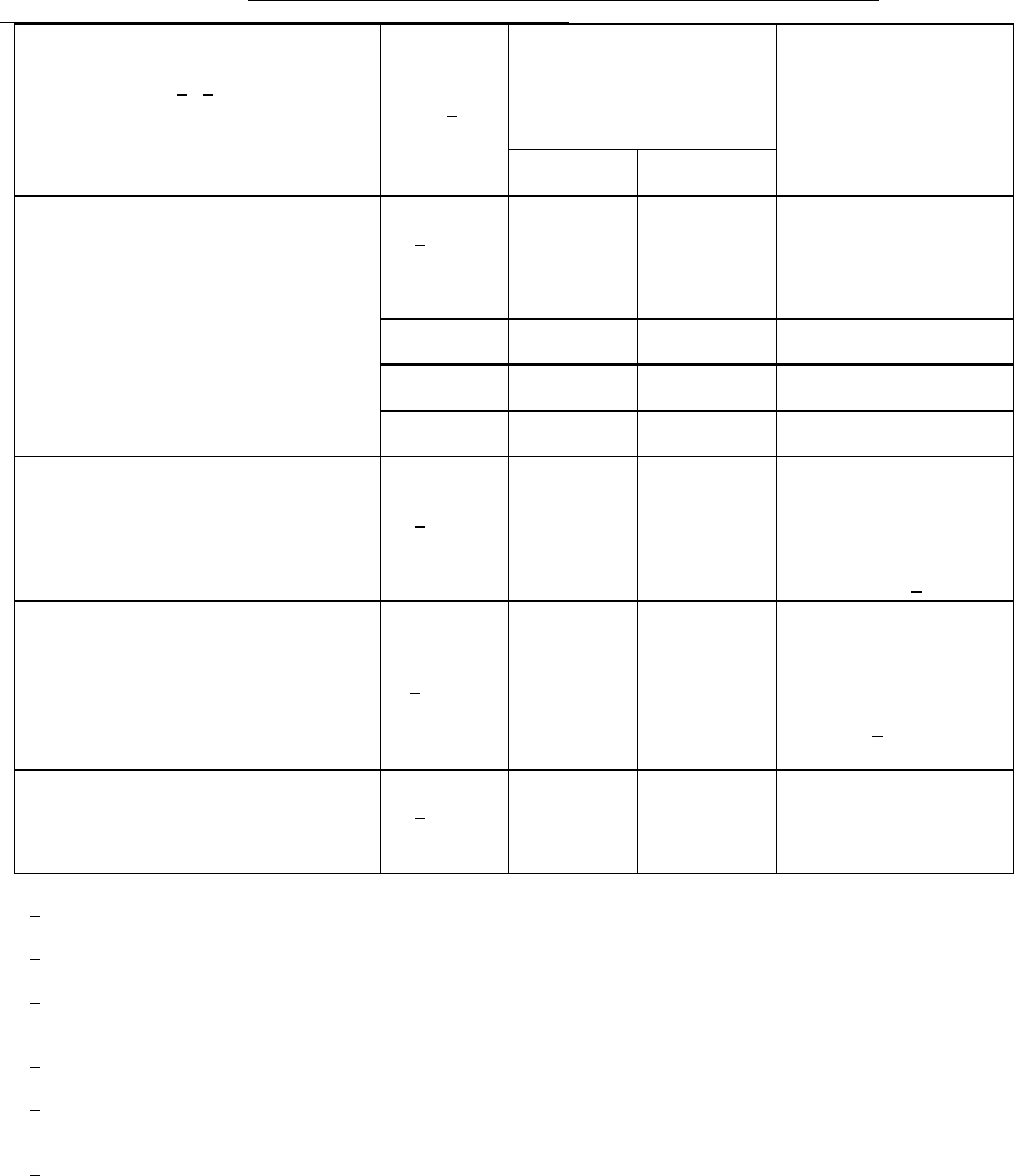
TABLE I. Wafer sampling procedures for various metallization chamber configurations.
Metallization chamber
configuration
1
/ 2/
Number of
wafer lots
in chamber
3
/
Required number of
samples per wafer lot
Sampling plans
per wafer lot
Evaporation Sputtering
Projected plane view of the
Wafer-holder is a circle.
Wafer-holder is stationary
or "wobbulates"
1
4
/
5 2 Four from near the
periphery of the wafer-
holder and 90° apart.
One from the center of
holder. See figure 4.
2 3, 4, or 5 2 See figure 4.
3 3 or 4 2 See figure 4.
4 3 2 See figure 4.
Wafer-holder is symmetrical
(i.e., circular, square, etc.).
Deposition source(s) is above or below
the wafer-holder. Wafer-holder
rotates about its center during
deposition.
1, 2, 3,
or 4
4
/
2 2 For each wafer lot, one
from the periphery of the
wafer-holder, and one
from close proximity to
the center of rotation.
See figure 4. 5
/
Planetary system. One or more
symmetrical wafer-holders (planets)
rotate about their own axes while
simultaneously revolving about the
center of the chamber. Deposition
source(s) is above or below
the wafer-holders.
1, 2, 3,
or 4 per
planet
4
/
2 2 For each wafer lot, one
from near the periphery
of a planet and one from
near the center of the
same planet. See
figure 4. 6
/
Continuous feed. Wafers are
continuously inserted into deposition
chamber through a separate pump down
of an airlock (25 wafer nominal load)
1
1
/
2 2 Two randomly selected
wafers from each wafer
lot.
1
/ In this case, a wafer lot shall be defined as a batch of wafers which have received together those common processes
which determine the slope and thickness of the passivation steps on these wafers.
2
/ If a wafer-holder has only one circular row, or if only one row is used on a multi-rowed wafer-holder; the total number
of specified sample wafers shall be taken from that row.
3
/ If there is more than one wafer lot in a metallization chamber, each wafer lot shall be grouped approximately in a
separate sector within the wafer-holder. A sector is an area of the circular wafer-holder bounded by two radii and the
subtended arc; quadrants and semicircles are used as examples on figure 4.
4
/ If the wafer lot size exceeds the loading capacity of the metallization system each processed sub-lot will be sampled
as if it was a unique lot.
5
/ When evaluation data shows that there is no relationship between SEM results and the physical location of the
wafers during the metallization process. It shall be permissible to substitute two randomly selected wafers from each
wafer lot. This analysis shall be repeated after each major equipment repair.
6
/ Sample wafers need be selected from only one planet if all wafer lots contained in the chamber are included in that
planet. Otherwise, sample wafers of the wafer lot(s) not included in that planet, shall be selected from another
planet(s).