MIL- STD-883F 2004 TEST METHOD STANDARD MICROCIRCUITS.pdf - 第319页
MIL-STD-883F METHOD 2018.4 18 June 2004 7 3.6 Acc eptance r equirement s . 3.6.1 Si ngle wafer ac cept ance basi s . The metal lizati on on a singl e wafer s hall be judged ac ceptabl e only if all t he sampled ar eas or…
MIL-STD-883F
METHOD 2018.4
18 June 2004
6
3.5.1.2 Barrier/adhesion layers. The examination of barrier/adhesion layers designed to conduct less than 10% of the
total current is not required as this is considered a non-conduction layer.
3.5.1.2.1 Barrier/adhesion layer as a conductor
. The barrier/adhesion layer shall be considered as a conductor
(considering the layer thickness and relative conductivity) provided that the following conditions are satisfied: At least ten
percent of the current is designed to be carried by this layer; and this layer is used in the current density calculations. When
this occurs the barrier/ adhesion layer and/or the principal conducting layer shall satisfy all of the step coverage
requirements collectively as baselined by the manufacturer. Specimen examination shall be in accordance with 3.5 and the
accept/reject criteria as defined in 3.7.1. The barrier/adhesion layer(s) shall be examined using either the SEM or optical
microscope. The following methods may be used to examine these barrier/adhesion layers:
3.5.1.2.1.1 The Etchback procedure
. This involves the stripping of each successive unique layer of metal by selective
etching, with suitable etchants, layer by layer, to enable the examination of each layer. Typically, each successive layer of
metal will be stripped in sequence to expose the next underlying layer for examination. Successive layer removal on a
single die area may be impractical. In this case the wafer area or additional die (dice) immediately adjacent on the slice to
the original die area shall be stripped to meet the requirement that all unique layers shall be exposed and examined.
3.5.1.2.1.2 In-line procedure
. The wafer(s) shall be inspected for the defined accept/reject criteria immediately after
being processed through each unique deposition and corresponding etching operation.
3.5.2 Passivation steps
. Inspect the metallization at all types of passivation steps in accordance with the requirements of
3.5.1.1 and table II.
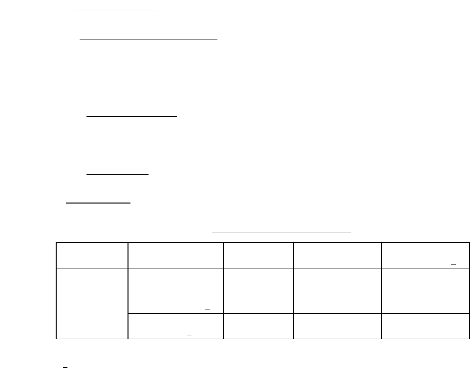
TABLE II. Examination procedure for specimens
.
Device type
Area of
examination
Examination Minimum-maximum
magnification
Photographic
documentation 1
/
Integrated
circuit devices
Passivation steps
(contact windows and
other types of
passivation steps) 2
/
At least one of
each type of
passivation
step present
5,000X to 50,000X Two of the worst
case passivation
steps
General
metallization 2
/
25 percent 1,000X to 6,000X Worst case general
metallization
1
/ See 3.8 (an additional photograph may be required).
2
/ See 3.7 for accept/reject criteria.
*
*
*
*
*
MIL-STD-883F
METHOD 2018.4
18 June 2004
7
3.6 Acceptance requirements.
3.6.1 Single wafer acceptance basis
. The metallization on a single wafer shall be judged acceptable only if all the
sampled areas or dice from that wafer are acceptable.
3.6.2 Wafer lot acceptance basis
. An entire wafer lot shall be judged acceptable only when all the sampled areas or dice
from all sample wafers are acceptable. If a wafer lot is rejected in accordance with this paragraph each wafer from that
wafer lot may be individually examined; acceptance shall then be in accordance with 3.6.1.
3.7 Accept/reject criteria
. Rejection of dice shall be based on batch process defects and not random defects such as
scratches, smeared metallization, tooling marks, etc. In the event that the presence of such random defects obscures the
detailed features being examined, an additional adjacent sample shall be inspected. Illustrations of typical defects are
shown in figures 2018-6 through 2018-22.
3.7.1 General metallization
. Any evidence of poor metallization adhesion shall be unacceptable. Any defects (see figure
2018-18 and 2018-20), such as voids, cracks, separations, depressions, notches, or tunnels, which singly or in combination
reduce the cross-sectional area of the general metallization stripe by more than 50 percent shall be unacceptable. Two
specific cases of general metallization are specified below:
3.7.1.1 Conductor stripes
. In the examination of the other metal layers for the specific case of conductor stripes
(exclusive of the contact window area), a defect consuming 100 percent of the thickness of the barrier/adhesion stripe shall
be acceptable provided that the defect does not extend more than 50 percent across the width of the metallization stripe
(see figure 2018-22).
3.7.1.2 Barrier layers in contact window areas
. No defects of any kind in a barrier layer which would bring the overlying
metal layer in contact with the semiconductor material surface shall be permitted.
3.7.1.3 Overlying adhesion layers
. For the metal layer(s) above the principal conducting layer, a defect consuming 100
percent of the thickness of the adhesion stripe shall be acceptable provided that the defect does not extend more than 50
percent across the width of the metallization stripe.
3.7.2 Passivation steps
. Metallization over a passivation step shall be unacceptable if any combination of defects (see
figure 2018-23) or thinning of the metal reduces the cross-sectional area of the metallization stripe along any cross-sectional
plane in a major current-carrying direction to less than 50 percent of the cross-sectional area of the stripe. A minimum of 20
percent total metallization coverage (barrier metal inclusive, see figure 2018-24) in the primary current carrying direction will
be allowed for metallization over a passivation step when the structure involved is a circular or multisided via or contact
structure and there is sufficient wrap-around metal (>10 percent of incoming metal line width) to allow for current flow to all
sides of the via or contact. The metallization must meet the current density requirements of MIL-PRF-38535. In cases
where an absence of visible edge or a smooth transition or taper clearly reveals effective coverage, a cross-section will be
performed to verify metal coverage.
3.7.2.1 Nonrejectable cross-sectional area
. In the event that the metallization cross-sectional area at a particular directional
edge profile is less than as allowed in 3.7.2. This shall not be cause for rejection if the following two conditions occur:
*
*
MIL-STD-883F
METHOD 2018.4
18 June 2004
8
3.7.2.1.1 Condition 1. It is determined that the directional edge profile from which metal is absent does not occur in the
major current-carrying directional edge. Such determination shall be made either by scanning all passivation steps of this
type on the remainder of the die, or by the examination of a topographical map supplied by the manufacturer which shows
the metal interconnect pattern.
3.7.2.1.2 Condition 2
. Acceptance shall be on a single wafer basis only.
3.7.2.2 Nonrejectable, noncovered directional edge
. For passivation steps to be acceptable, all directional edges shall be
covered with metallization and be acceptable to the requirements of 3.7.2.1, unless by design. In the event that a directional
edge profile of a particular type of passivation step is not covered with metallization, this shall not be cause for rejection if
the following two conditions occur:
3.7.2.2.1 Condition 1
. It is determined that the directional edge profile from which metal is absent does not occur in the
major current-carrying directional edge. Such determination shall be made either by scanning all passivation steps of this
type on the remainder of the die, or by the examination of a topographical map supplied by the manufacturer which shows
the metal interconnect pattern.
3.7.2.2.2 Condition 2
. None of the other specimens from the sampled wafers representing the lot exhibit a directional
edge profile from which metal is absent in the major current-carrying directional edge.
NOTE: If both 3.7.2.2.1 and 3.7.2.2.2 are satisfied, a wafer lot acceptance basis shall be used. However, if only 3.7.2.2.1 is
satisfied, a single wafer acceptance basis shall be used.
3.7.3 Verification of potential rejects
. At the option of the manufacturer, it shall be permissible to subject the specimen, or
an adjacent sample that exhibits the same reject mode, to a verification test. Given below are some examples of suitable
verification tests:
3.7.3.1 Cross-sectioning
. A passivated sample shall be cleaved or lapped down to bisect the area of concern. The
sample may then be subjected to an etchant that will remove the interconnecting metallization at the inspection surface (i.e.,
approximately perpendicular to the die surface). Specimens may be examined without any special surface coating if surface
charging is not a significant problem and adequate resolution and signal-to-noise levels are obtained. If the specimens are
coated, they shall be coated with a thin vapor-deposited or sputtered film of a suitable conductive material (i.e., 100Å gold).
The coating deposition processes shall be controlled such that no artifacts are introduced by the coating. The sample shall
be prepared (see 3.3) and examined in the SEM for interconnect metallization thickness or percentage coverage at the
passivation step, or any other relevant parameter. Note: This cross-sectioning technique is not conclusive for hairline
microcracks as they are not adequately filled by the passivation material.
3.7.3.1.1 Dimensional errors
. Care must be taken to ensure that the cross-section is close to the center of a contact in
order to avoid dimensional errors due to the rounding of the contact corners.
3.7.3.2 Surface etchback
. The unpassivated sample surface is subjected to a chemical etch which removes the
interconnection metallization from the surface of the die at a known controlled rate. The etching is stopped when the
required metal thickness has been removed. The sample is then prepared (see 3.3) and examined within the SEM for
residual metal at the passivation step/contact window interface. Photographic evidence shall then be taken of the sample(s)
to support the acceptance or rejection of the material.
3.7.3.3 Topographical integration
. A graphical representation of the worst case cross-sectional area is drawn to scale on
appropriate graph paper from comprehensive photographs taken eucentrically about the directional edge. The
cross-sectional area is then graphically integrated. This technique is useful for evaluating metallization with irregular surface
topography.
3.8 Specimen documentation requirements
. A minimum of three photographs for each layer of each level of metallization
inspected per lot shall be taken and retained for a minimum of five years after performance of the inspection. Two
photographs shall be of worst case passivation steps and the third photograph of worst case general metallization. If any
photograph shows an apparent defect within the field of view, another photograph shall be taken to certify the extent of the
apparent defect (see table II).
*
*
*
*
*
*