MIL- STD-883F 2004 TEST METHOD STANDARD MICROCIRCUITS.pdf - 第362页
MIL-STD-883F METHOD 2020.8 18 June 2004 6 This page i ntenti onally lef t blank
MIL-STD-883F
METHOD 2020.8
18 June 2004
5
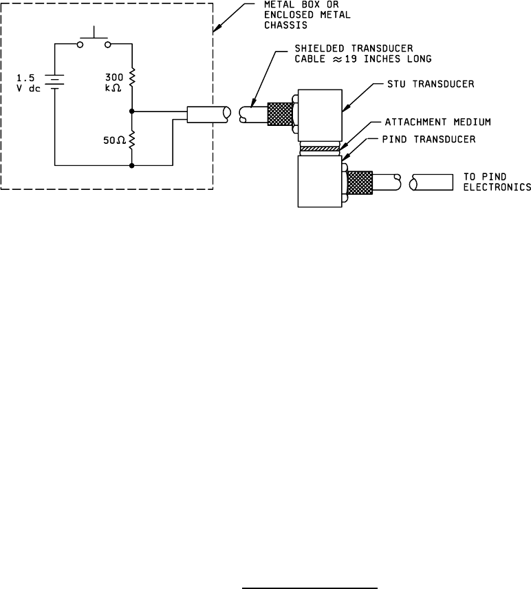
NOTES:
1. Pushbutton switch: Mechanically quiet, fast make, gold contacts. E.G. T2 SM4 microswitch.
2. Resistance tolerance 5 percent noninductive.
3. Voltage source can be a standard dry cell.
4. The coupled transducers must be coaxial during test.
5. Voltage output to STU transducer 250 microvolts, ±20 percent.
FIGURE 2020-1 Typical sensitivity test unit
.
MIL-STD-883F
METHOD 2020.8
18 June 2004
6
This page intentionally left blank

MIL-STD-883F
METHOD 2021.3
29 November 1985
1
METHOD 2021.3
GLASSIVATION LAYER INTEGRITY
1. PURPOSE
. The purpose of this test is to assess the structural quality of deposited dielectric films (e.g., CVD,
sputtered or electron beam evaporated glass or nitride, etc.) over aluminum metallized semiconductor devices or
microcircuits. The test is directed at identifying process and materials related glass layer defects which result in localized
contamination buildup and loss of the advantage given to properly glassivated devices in terms of electromigration behavior
at elevated temperature and current density. This is a destructive test.
2. APPARATUS
. The apparatus for this test shall consist of suitable sample handling and chemical etching facilities as
required for personnel safety. Standard optical microscopes such as those employed in method 2010 shall be used for
device inspection. Standard A.C.S. Reagent Grade chemicals shall be used as etchant materials.
3. PROCEDURE
. Unless otherwise specified, this test shall be applied to devices which have been through the complete
assembly cycle including final package seal. Packaged devices shall be mechanically delidded with minimum thermal
stresses applied. Unless otherwise specified, the test sample shall consist of a minimum of one device selected randomly
from the inspection lot. One of the following etching procedures shall be used.
3.1 Procedure A
. Delidded sample devices shall be completely immersed in the following aluminum etch:
40 Volumes H
3
PO
4
(85%)
19 Volumes H
2
0
4 Volumes HNO
3
(70%)
This solution shall be maintained at a temperature of 50°C ±5°C.
Devices shall be examined during the etching procedure with an optical system, such as a monocular, binocular or
stereomicroscope compatible with observation of the immersed samples. Devices shall be etched for twice the amount of
time required to completely remove aluminum metallization from exposed bonding pads.
Properly etched devices shall be removed from the heated solution, rinsed in distilled water, and blown dry with compressed
air or other suitable gas streams.
Final optical inspection after etching and drying shall be performed at a magnification of 100X minimum.
3.2 Procedure B
. Delidded sample devices shall be completely immersed for 20 to 30 minutes at room temperature in
the following aluminum etch:
5 Volumes HN0
3
(70%)
80 Volumes H
3
P0
4
(85%)
5 Volumes Acetic Acid
10 Volumes Deionized Water
NOTE: The use of a commercial equivalent (e.g., Mity Etch 2) is acceptable.
Properly etched devices shall be removed from the solution, rinsed in distilled water, and blown dry with compressed air or
other suitable gas streams.
Final optical inspection after etching and drying shall be performed at a magnification of 100X minimum.