MIL- STD-883F 2004 TEST METHOD STANDARD MICROCIRCUITS.pdf - 第404页
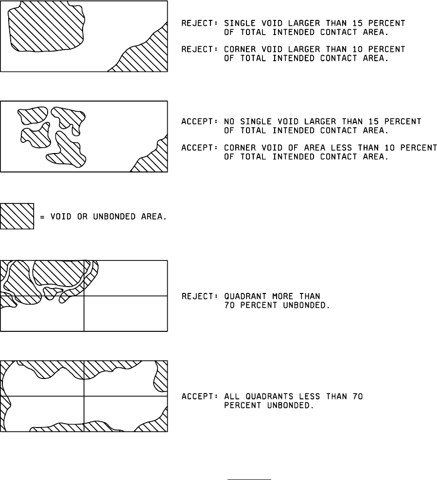
MIL-STD-883F METHOD 2030 29 May 1987 4 FI GURE 2030-1. Voi d cri teria .
MIL-STD-883F
METHOD 2030
29 May 1987
3
3.6 Reports of records.
3.6.1 Reports of inspection
. For class level S devices, or when specified for other device class levels, the manufacturer
shall furnish inspection reports with each shipment of devices. The report shall describe the results of the ultrasonic
inspection, and list the purchase order number or equivalent identification, the part number, the date code, the quantity
inspected, the quantity rejected, and the date of test. For each rejected device, the part number, the serial number when
applicable, and the cause for rejection shall be listed.
3.6.2 Acoustic micrograph and report retention
. When specified, the manufacturer shall retain a set of the ultrasonic
images and a copy of the inspection report. These shall be retained for the period specified.
3.7 Examination and acceptance criteria
. In the examination of devices, the following aspects shall be considered
unacceptable die mounting, and devices that exhibit any of the following defects shall be rejected.
Voids: When imaging devices ultrasonically, certain types of mounting material may not give true representation of voids.
When such devices are inspected, the mounting shall be noted on the inspection report.
a. Contact area voids in excess of 50 percent of the total intended contact area.
b. A single void which exceeds 15 percent of the intended contact area, or a single corner void in excess of 10
percent of the total intended contact area (see figure 2030-1).
c. When the image is divided into four equal quadrants by bisecting both pairs of opposite edges, any quadrant
exhibiting contact area voids in excess of 70 percent of the intended quadrant contact area (see figure 2030-1).
In case of dispute, the percent of voiding shall be determined by actual measurement from the image.
4. SUMMARY
. The following details shall be specified in the applicable acquisition document:
a. Number of views, if other than indicated in 3.1.1.
b. Marking, if other than indicated in 3.2 and marking of samples to indicate they have been ultrasonically imaged, if
required.
c. Defects to be sought in the samples and criteria for acceptance or rejection, if other than indicated in 3.7.
d. Image and report retention, if applicable (see 3.6.2).
e. Test reports when required for class level B devices.
MIL-STD-883F
METHOD 2030
29 May 1987
4
FIGURE 2030-1. Void criteria
.

MIL-STD-883F
METHOD 2031.1
27 July 1990
1
METHOD 2031.1
FLIP-CHIP PULL-OFF TEST
1. PURPOSE
. The purpose of this test is to measure the strength of internal bonds between a semiconductor die and a
substrate to which it is attached in a face-bond configuration.
2. APPARATUS
. The apparatus for this test shall consist of suitable equipment for applying the specified stress to the
bonds. A calibrated measurement and indication of the applied stress in grams force (gf) shall be provided by equipment
capable of measuring stresses up to twice the specified minimum limit value, with an accuracy of ±5 percent or ±0.25 gf,
whichever is the greater tolerance.
3. PROCEDURE
. The test shall be conducted using the following procedure. All die pulls shall be counted and the
specified sampling, acceptance, and added sample provisions shall be observed, as applicable. The sample size number
and accept number specified shall determine the number of die to be tested (not bonds). For hybrid or multichip devices, a
minimum of 4 die or all die if four are not available on a minimum of 2 completed devices shall be used. All pull tests shall
be performed prior to the application of encapsulants, adhesive, or any material which may increase the apparent bond
strength.
When flip chips are bonded to substrates other than those in completed devices, the following conditions shall apply:
a. The sample of chips for this test shall be taken at random from the same chip population as that used in the
completed devices that they are intended to represent.
b. The chips for this test shall be bonded on the same bonding apparatus as the completed devices, during the time
period within which the completed devices are bonded.
c. The test chip substrates shall be processed, metallized, and handled identically with the completed device
substrates, during the same time period within which the completed device substrates are processed.
3.1 Testing
. The calibrated pull-off apparatus (see 2) shall include a pull-off rod (for instance, a current loop of nichrome
or Kovar wire) having a cross-sectional area of 75 percent, +3 percent, -5 percent of the chip surface area. The rod shall
make connection with a hard setting adhesive material (for instance, a cyanoacrylate or other adhesive possessing high
tensile strength) on the back of the flip chip. The substrate shall be rigidly installed in the pull-off fixture and the pull-off rod
shall make firm mechanical connection to the adhesive material. The die shall be pulled without shock, within 5° of the
normal at a rate of 500 grams ±100 grams per second, until the die separates from the substrate. When a failure occurs,
the force at the time of failure, the calculated force limit, and the failure category shall be recorded.
3.2 Failure criteria
. Any flip-chip pull which results in separation under an applied stress less than
500 kg/in
2
x average solder bump area (in
2
) x number of solder bumps shall constitute a failure.
3.2.1 Failure category
. Failure categories are as follows: When specified, the stress required to achieve separation and
the predominant category of separation or failure shall be recorded.
a. Silicon broken.
b. Lifted metallization from chip.
c. Separation at bond-chip interface.
d. Failure within bond.