MIL- STD-883F 2004 TEST METHOD STANDARD MICROCIRCUITS.pdf - 第410页
MIL-STD-883F METHOD 2032.2 18 June 2004 4 (16) Mar is a nontear ing sur fac e dist urbance s uch as an i ndentati on or a buff mark. (17) Metalliza tion, mu ltilevel (c onductors ) is al ternat e layers of metall izati o…
MIL-STD-883F
METHOD 2032.2
18 June 2004
3
(6) Contact window is an opening (usually square) through the oxide (or insulating) layer for the purpose of
allowing contact by deposited material to the substrate.
(7) Controlled environment
is one that has 1,000 or fewer (0.5 Hm or greater) particles/cubic foot in a controlled
environment in accordance with the requirements of ISO 14644-1 for a class 6 clean environment, except
that the maximum allowable relative humidity shall not exceed 65 percent.
(8) Corrosion
is the gradual wearing away of metal, usually by chemical action, with the subsequent production
of a corrosion product.
(9) Crazing
is the presence of numerous, minute, interconnected surface cracks.
(10) Crossover
is the transverse crossing of metallization paths, without mutual electrical contact, achieved by
the deposition of an insulating layer between the metallization paths in the area of crossing.
(11) Detritus
is fragments of original or trim-modified resistor or conductor material.
(12) Dielectric
is an insulating material that does not conduct electricity but may be able to sustain an electric
field. It can be used in crossovers, as a passivation or a glassivation, or in capacitors.
(13) Foreign material
is any material that is foreign to the element or any nonforeign material that is displaced
from its original or intended position in the element. It is considered attached when it cannot be removed by
a nominal gas blow (approximately 20 psig) or by an approved cleaning process. Conductive foreign
material is any substance that appears opaque under those conditions of lighting and magnification used in
routine visual inspection. Particles are considered to be embedded in glassivation when there is evidence of
color fringing around the periphery of the particle.
(14) Glassivation
is the top layer(s) of transparent insulating material that covers the active circuit area, including
metallization, but not bonding pads. Crazing is the presence of numerous minute cracks in the glassivation.
Cracks are fissures in the glassivation layer resulting from stress release or poor adhesion. The cracks can
form loops over metallized areas.
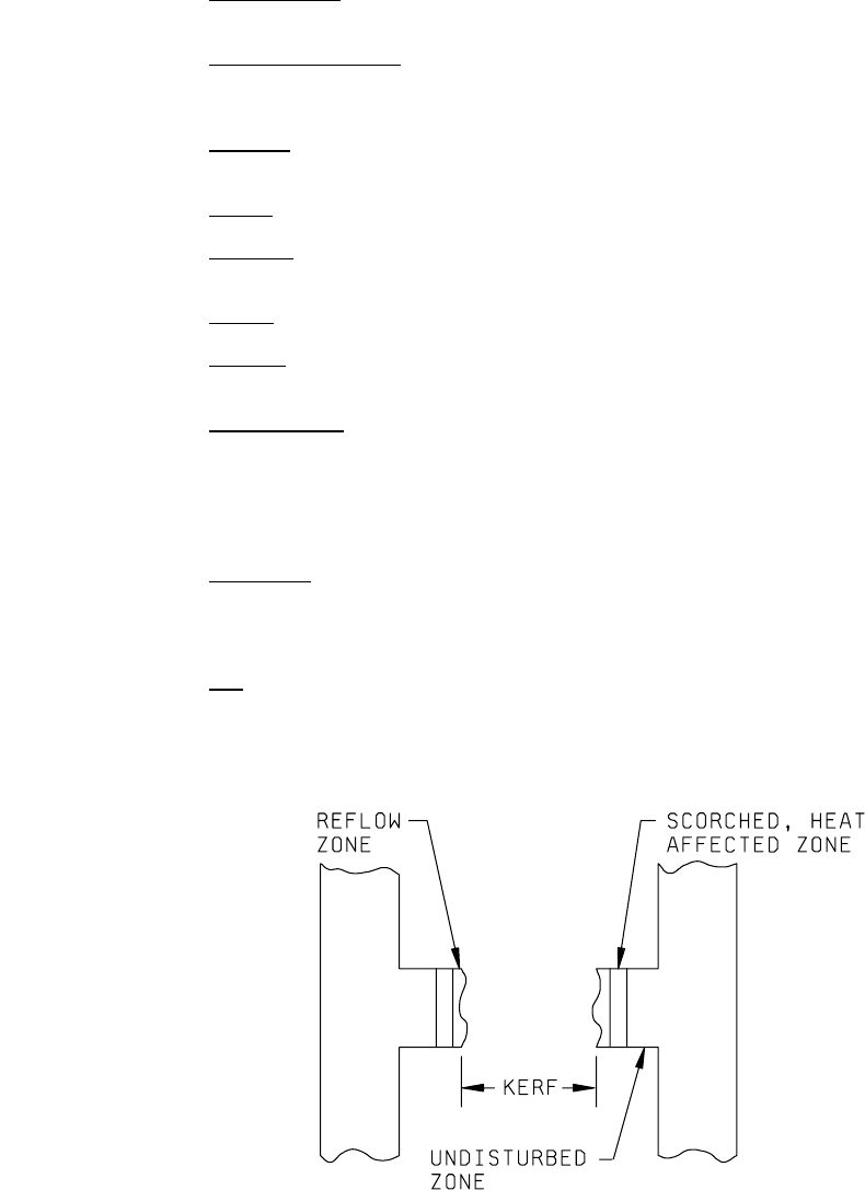
(15) Kerf
is the clear area in a trimmed resistor resulting from the removal of resistor material by the trimming
operation. In laser trimming, the kerf is bounded by the reflow zone (which is characterized by adherent,
melted resistor material), the scorched heat-affected zone (which is characterized by discoloration of the
resistor film without alteration of its physical form), and the undisturbed zone.
*
MIL-STD-883F
METHOD 2032.2
18 June 2004
4
(16) Mar is a nontearing surface disturbance such as an indentation or a buff mark.
(17) Metallization, multilevel (conductors)
is alternate layers of metallization, or other material used for
interconnection, that are isolated from each other by a grown or deposited insulating material. The term
"overlaying metallization" refers to any metallization layer on top of the insulating material.
(18) Metallization, multilayered (conductors)
is two or more layers of metallization, or other material used for
interconnection, that are not isolated from each other by a grown or deposited insulating material. The term
"underlying metallization" refers to any metallization layer below the top layer of metallization.
(19) Metallization, operating (conductors)
is all metallization (gold, aluminum, or other material) used for
interconnection. Bonding pads are considered to be operating metallization. Alignment markers, test
patterns, and identification markings are not considered to be operating metallization.
(20) Narrowest resistor width
is the narrowest portion of a given resistor prior to trimming; however, the
narrowest resistor width for a block resistor may be specified in the approved manufacturer's design
documentation.
(21) Neck-down
is tapering of a resistor line at a metallization interface. Resistor material taper is typically equal
on both sides of the line and is less abrupt than a void.
(22) Nicking (partial cut)
is incomplete or inadvertent trimming of a resistor adjacent to the one being trimmed or
of the next ladder rung of the same resistor.
(23) Nonplanar element
is one that is essentially three-dimensional.
(24) Original separation
is the separation dimension or space that is intended by design.
(25) Original width
is the width dimension that is intended by design.
(26) Oxide defect
is an irregularly shaped defect in the oxide characterized by two or three colored fringes at it
edges.
(27) Passivation
is the silicon oxide, silicon nitride, or other insulating material, that is grown or deposited directly
on the element prior to the deposition of metal.
(28) Passivation step
is a change in thickness of the passivation layer by design.
(29) Passive elements
are planar resistors, capacitors, inductors, and patterned substrates (both single-layer
and multilayer), and nonplanar chip capacitors, chip resistors, chip inductors, and transformers.
(30) Patterned substrate
is a substrate on which conductors, and components such as resistors or capacitors,
are formed using thick or thin film manufacturing techniques.
(31) Planar element
is one that is essentially two-dimensional with all points in a common plane.
(32) Protrusion
is a jutting-out of a circuit feature. Protrusion is typically caused by a photolithographic or
screening defect.
(33) Resistor ladder
is a resistor structure resembling a ladder in appearance that can be trimmed in incremental
steps. A coarse ladder structure is one in which trimming of a rung results in a large incremental resistance
change (one that can cause an out-of-tolerance condition to occur). A fine ladder structure is one in which
trimming of a rung results in a small incremental resistance change (one that can not cause an
out-of-tolerance condition to occur).
MIL-STD-883F
METHOD 2032.2
18 June 2004
5
(34) Resistor ladder rung is that portion of a resistor ladder structure intended to be laser trimmed to result in an
incremental change in resistance.
(35) Resistor loop
is a resistor structure resembling a loop in appearance that can be trimmed. A coarse loop
structure is one in which trimming results in a large resistance change (one that can cause an
out-of-tolerance condition to occur). A fine loop structure is one in which trimming results in a small
resistance change (one that cannot cause an out-of-tolerance condition to occur).
(36) Resistor material, self passivating
is one on which a conformal insulating layer can be thermally grown (such
as tantalum nitride on which tantalum pentoxide is grown).
(37) Scorching
is discoloration of laser trimmed thin film resistor material without alteration of its physical form.
(38) Scratch, metallization
is any tearing defect, including probe marks, in the surface of the metallization. A mar
on the metallization surface is not considered to be a scratch.
(39) Scratch, resistor
is any tearing defect in the resistor film. A mar on the resistor surface is not considered to
be a scratch.
(40) Sidebar
is that portion of a resistor ladder structure to which rungs are attached. Sidebars are not intended
to be laser trimmed.
(41) Substrate
is the supporting structural material into or upon which, or both, functional circuits are formed.
(42) Surface Acoustic Wave (SAW) element
is a planar element fabricated typically using thin film manufacturing
techniques on various substrate materials. Size varies as a function of frequency and design features
include interdigitated fingers.
(43) Terminal
is a metal area used to provide an electrical access point to functional circuitry.
(44) Thick film
is conductive, resistive or dielectric material screen printed onto a substrate and fired at
temperature to fuse into its final form.
(45) Thin film
is conductive, resistive or dielectric material, usually less than 50,000Å in thickness, that is
deposited onto a substrate by vacuum evaporation, sputtering, or other means.
(46) Underlying material
is any layer of material below the top-layer metallization. This includes metallization,
resistor, passivation or insulating layers, or the substrate itself.
(47) Via
is an opening in the insulating material in which a vertical conductive electrical connection from one
metallization layer to another is made.
(48) Vitrification
is conversion into glass or a glassy substance by heat and fusion.
(49) Void, metallization
is any missing metallization where the underlying material is visible (exposed). Voids
typically are caused by photolithographic, screen, or mask related defects, not by scratches.
(50) Void, resistor
is any missing resistor material where the underlying material is visible (exposed). Voids
typically are caused by photolithographic, screen, or mask related defects, not by scratches.