MIL- STD-883F 2004 TEST METHOD STANDARD MICROCIRCUITS.pdf - 第412页
MIL-STD-883F METHOD 2032.2 18 June 2004 6 (51) W rapar ound conduct or is one which extends around the edge of the subs trat e by design. (52) Coupling (ai r) br idge is a r aised l ayer of met allizat ion used f or int …

MIL-STD-883F
METHOD 2032.2
18 June 2004
5
(34) Resistor ladder rung is that portion of a resistor ladder structure intended to be laser trimmed to result in an
incremental change in resistance.
(35) Resistor loop
is a resistor structure resembling a loop in appearance that can be trimmed. A coarse loop
structure is one in which trimming results in a large resistance change (one that can cause an
out-of-tolerance condition to occur). A fine loop structure is one in which trimming results in a small
resistance change (one that cannot cause an out-of-tolerance condition to occur).
(36) Resistor material, self passivating
is one on which a conformal insulating layer can be thermally grown (such
as tantalum nitride on which tantalum pentoxide is grown).
(37) Scorching
is discoloration of laser trimmed thin film resistor material without alteration of its physical form.
(38) Scratch, metallization
is any tearing defect, including probe marks, in the surface of the metallization. A mar
on the metallization surface is not considered to be a scratch.
(39) Scratch, resistor
is any tearing defect in the resistor film. A mar on the resistor surface is not considered to
be a scratch.
(40) Sidebar
is that portion of a resistor ladder structure to which rungs are attached. Sidebars are not intended
to be laser trimmed.
(41) Substrate
is the supporting structural material into or upon which, or both, functional circuits are formed.
(42) Surface Acoustic Wave (SAW) element
is a planar element fabricated typically using thin film manufacturing
techniques on various substrate materials. Size varies as a function of frequency and design features
include interdigitated fingers.
(43) Terminal
is a metal area used to provide an electrical access point to functional circuitry.
(44) Thick film
is conductive, resistive or dielectric material screen printed onto a substrate and fired at
temperature to fuse into its final form.
(45) Thin film
is conductive, resistive or dielectric material, usually less than 50,000Å in thickness, that is
deposited onto a substrate by vacuum evaporation, sputtering, or other means.
(46) Underlying material
is any layer of material below the top-layer metallization. This includes metallization,
resistor, passivation or insulating layers, or the substrate itself.
(47) Via
is an opening in the insulating material in which a vertical conductive electrical connection from one
metallization layer to another is made.
(48) Vitrification
is conversion into glass or a glassy substance by heat and fusion.
(49) Void, metallization
is any missing metallization where the underlying material is visible (exposed). Voids
typically are caused by photolithographic, screen, or mask related defects, not by scratches.
(50) Void, resistor
is any missing resistor material where the underlying material is visible (exposed). Voids
typically are caused by photolithographic, screen, or mask related defects, not by scratches.
MIL-STD-883F
METHOD 2032.2
18 June 2004
6
(51) Wraparound conductor is one which extends around the edge of the substrate by design.
(52) Coupling (air) bridge
is a raised layer of metallization used for interconnection that is isolated from the
surface of the element by an air gap or other insulating material.
(53) Pit
is a depression produced in a substrate surface typically by nonuniform deposition of metallization or by
nonuniform processing such as excessively powered laser trim pulses.
(54) Substrate, hard
is the inorganic, rigid material into or upon which or both, functional circuits are formed.
Typical materials are alumina and silicon.
(55) Blister, metallization
is a hollow bump that can be flattened.
(56) Nodule, metallization
is a solid bump that cannot be flattened.
(57) Substrate plug via
is a cylinder-like volume in the substrate material filled with conductive material which
makes electrical connection from contact areas on the top surface to the back surface of the substrate..
3.1 Thin film element inspection
. Inspection for visual defects described in this section shall be conducted on each planar
thin film passive element. The "high magnification" inspection shall be within the range of 100X to 200X for both class H and
class K. The "low magnification" inspection shall be within the range of 30X to 60X for both class H and class K. When
inspection is performed prior to mounting, then elements utilizing ceramic or glass type substrates, without backside
metallization, shall be inspected using backlighting for conditions of hair-line voiding or bridging. Patterned substrates that
have geometries of 2.0 mils or greater shall be inspected at 10X to 60X magnification.
Class H
Class K
3.1.1 Operating metallization defects "high
magnification"
. No element shall be acceptable
that exhibits:
NOTE: The metallization defect criteria contained
in this section apply to operating metallization
only.
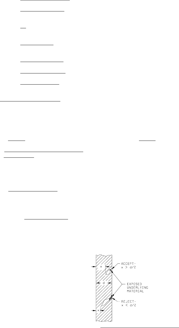
3.1.1.1 Metallization scratches
.
a. A scratch or probe mark in the metallization, a. Same as Class H.
excluding bonding pads, that both exposes
under-lying material anywhere along its length and
leaves less than 50 percent
of the original
metallization width undisturbed (see 2032-1h).
NOTE: These criteria do not apply to
capacitors (see 3.1.1.1e).
NOTE: Underlying material does not have to be
exposed along the full length of the scratch.
FIGURE 2032-1h. Class H metallization scratch criteria
.
MIL-STD-883F
METHOD 2032.2
18 June 2004
7
Class H
Class K
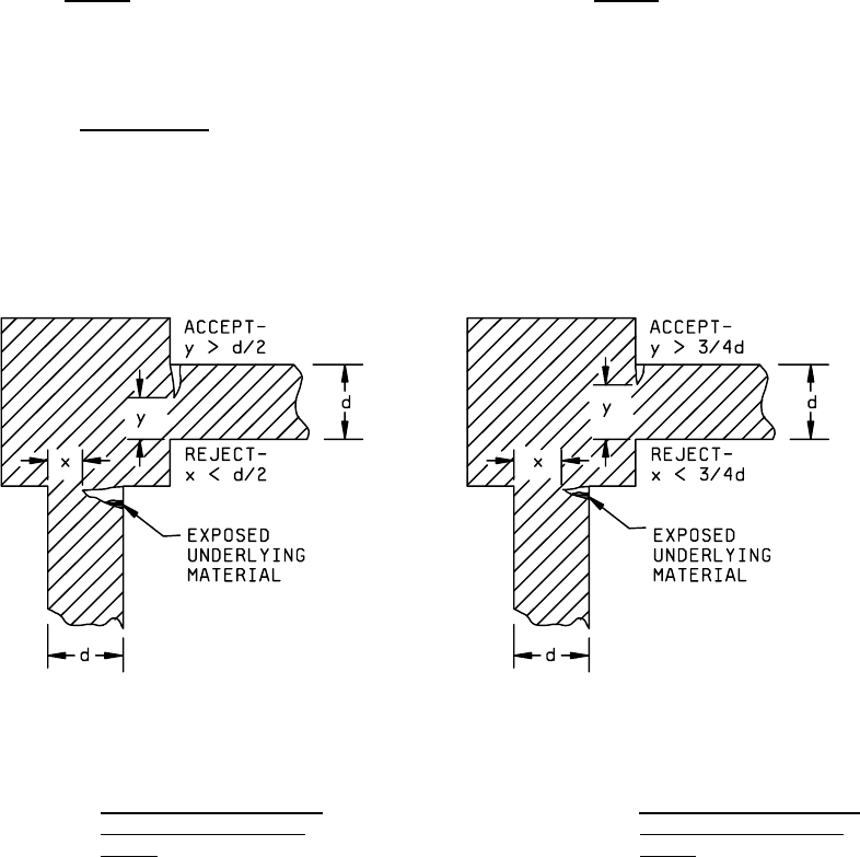
3.1.1.1 b. Scratch in the bonding pad area 3.1.1.1 b. Less than 75 percent (see
that both exposes underlying material and figure 2032-2k).
reduces the metallization path width,
where it enters the bonding pad, and leaves
less than 50 percent
of its original
metallization width. If two or more
metallization paths enter a bonding pad,
each shall be considered separately
(see figure 2032-2h).
FIGURE 2032-2h. Class H metallization width
FIGURE 2032-2k. Class K metallization width
reduction at bonding pad
reduction at bonding pad
criteria
. criteria.
3.1.1.1 c. Scratch that completely crosses a c. Same as class H.
Metallization path and damages the
surface of the surrounding
passivation, glassivation, or substrate on
either side.
d. Scratches or probe marks in the d. Same as class H.
bonding pad area that expose
underlying material over greater
than 25 percent of the original
unglassivated metallization area.
e .For capacitors only, a scratch in the e. Same as class H.
metallization, other than in the bonding
pad area, that exposes the dielectric
material.