MIL- STD-883F 2004 TEST METHOD STANDARD MICROCIRCUITS.pdf - 第424页
MIL-STD-883F METHOD 2032.2 18 June 2004 18 C lass H Class K 3.1.4 Subs trat e defect s "high magni fic ation" . No element s hall be ac ceptabl e that exhibit s: a. Less than 0.1 mi l of separ ation between a. …

MIL-STD-883F
METHOD 2032.2
18 June 2004
17
Class H Class K
3.1.3 b. Any lifting or peeling of the glassivation. 3.1.3 b. Same as class H.
NOTE: Lifting or peeling of the
glassivation is acceptable when it does not
extend more than 1.0 mil from the designed
periphery of the glassivation, provided that
the only exposure of metallization is of
adjacent bonding pads or of metallization
leading from those pads.
c. A void in the glassivation that exposes c. Same as class H.
two or more adjacent operating
metallization paths, excluding bonding
pad cutouts, unless by design.
d. Unglassivated nonactive circuit areas greater d. Same as class H.
than 5.0 mils in any dimension, unless by
design.
e. Unglassivated areas at the edge of a bonding e. Same as class H.
pad exposing the conductive substrate.
f. Glassivation covering more than 25 percent f. Same as class H.
of a bonding pad area.
g. Crazing in glassivation over a resistor. g. Same as class H.
h. Misalignment of the glassivation that h. Same as class H.
results in incomplete coverage of a
resistor, unless by design.
i. Glassivation scratches or voids that i. Same as class H.
expose any portion of a resistor or
fusible link except for polycrystalline
silicon links where the glassivation is
opened by design.
j. Scratches in the glassivation that disturb j. Same as class H.
metallization and bridge metallization
paths.
k. Cracks (not crazing) in the glassivation k. Same as class H.
that form a closed loop over adjacent
metallization paths.
MIL-STD-883F
METHOD 2032.2
18 June 2004
18
Class H Class K
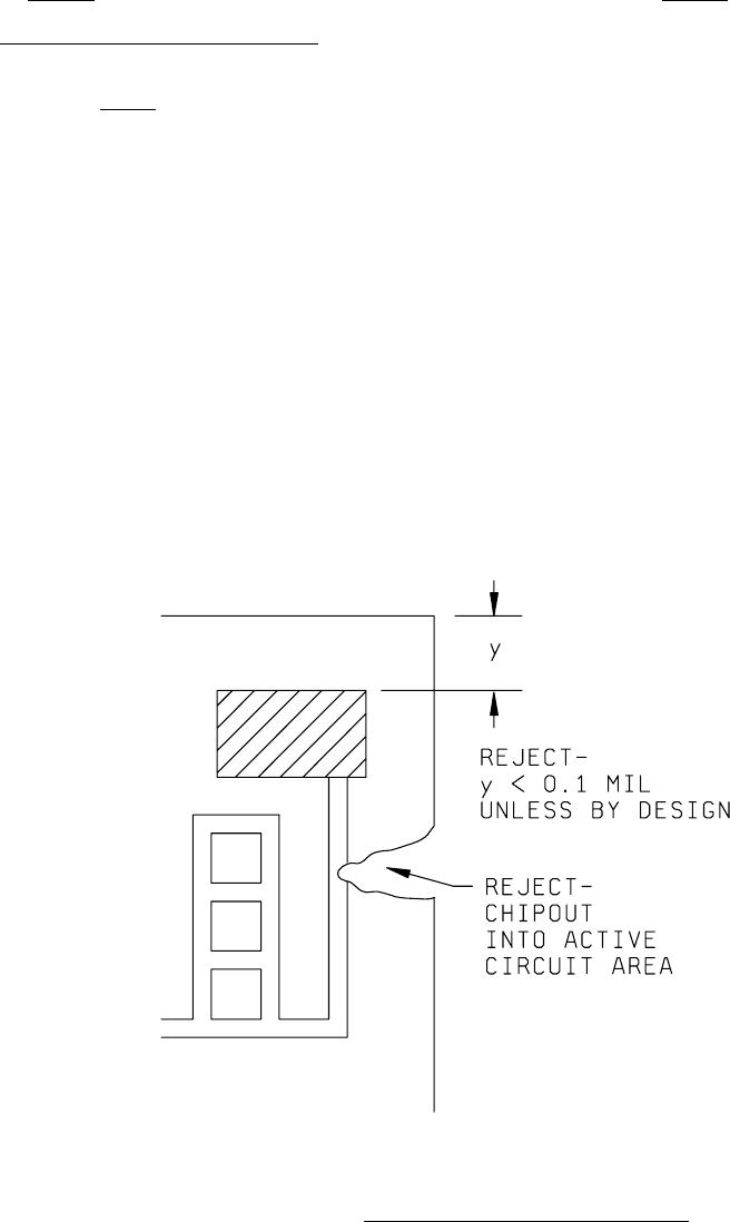
3.1.4 Substrate defects "high magnification"
.
No element shall be acceptable that exhibits:
a. Less than 0.1 mil
of separation between a. Same as Class H.
the operating metallization and the edge
of the element unless by design
(see figure 2032-10h).
NOTE: For elements containing
wraparound conductors or for bonding pads
of RF/microwave elements that are coincident
with the element edge (as documented
on the design drawing) this criteria does
not apply. When bond pad metallization is
coincident with the element edge, a
minimum separation of 1.0 mil shall exist
between the bonding pad metallization at
the element edge and any noncommon
conductive surface.
b. A chipout that extends into the active b. Same as class H.
circuit area (see figure 2032-10h).
FIGURE 2032-10h. Class H separation and chipout criteria
.
MIL-STD-883F
METHOD 2032.2
18 June 2004
19
Class H Class K
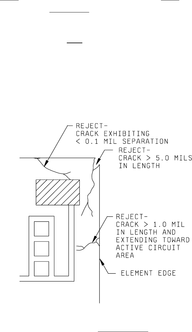
3.1.4 c. Any crack that exceeds 5.0 mils in length
3.1.4 c. Same as Class H.
(see figure 2032-11h).
NOTE: For fused quartz or crystalline
substrates, no cracking is allowed.
d. Any crack that does not exhibit 0.1 mil
d. 0.25 mil (see figure 2032-11k).
of separation from any active circuit
area or operating metallization (see
figure 2032-11h).
e. Any crack exceeding 1.0 mil in length e. Same as class H.
extending from the element edge directly
towards the active circuit area or
operating metallization (see figure
2032-11h).
FIGURE 2032-11h. Class H crack criteria
.