MIL- STD-883F 2004 TEST METHOD STANDARD MICROCIRCUITS.pdf - 第426页
MIL-STD-883F METHOD 2032.2 18 June 2004 20 Class H Cla ss K 3.1.4 f. N/A 3.1.4 f. Semici rcul ar cr ack or combinat ion of cracks al ong the element edge whos e total lengt h is equal to or gr eater t han 75 perc ent of …
MIL-STD-883F
METHOD 2032.2
18 June 2004
19
Class H Class K
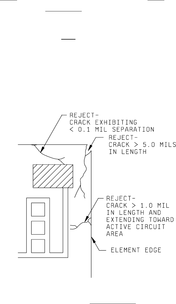
3.1.4 c. Any crack that exceeds 5.0 mils in length
3.1.4 c. Same as Class H.
(see figure 2032-11h).
NOTE: For fused quartz or crystalline
substrates, no cracking is allowed.
d. Any crack that does not exhibit 0.1 mil
d. 0.25 mil (see figure 2032-11k).
of separation from any active circuit
area or operating metallization (see
figure 2032-11h).
e. Any crack exceeding 1.0 mil in length e. Same as class H.
extending from the element edge directly
towards the active circuit area or
operating metallization (see figure
2032-11h).
FIGURE 2032-11h. Class H crack criteria
.
MIL-STD-883F
METHOD 2032.2
18 June 2004
20
Class H Class K
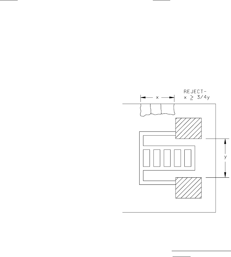
3.1.4 f. N/A 3.1.4 f. Semicircular crack or combination of
cracks along the element edge whose total
length is equal to or greater than 75
percent of the narrowest separation
between any two bonding pads (see figure
2032-12k).
FIGURE 2032-12k. Class K semicircular crack
criterion
.
g. An attached portion of an active circuit g. Same as class H.
area from an adjacent element.
h. Any crack that does not originate at an h. Same as class H.
edge.
i. Holes through the substrate, unless by i. Same as class H.
design.

MIL-STD-883F
METHOD 2032.2
18 June 2004
21
Class H Class K
3.1.5 Foreign material defects "low magnification"
.
No element shall be acceptable that exhibits:
a. For mounted elements, unattached, a. Same as class H.
conductive foreign material on the surface
of the elements. For unmounted elements,
unattached, conductive foreign material
on the surface of the element that is
large enough to bridge operating
metallization paths, active circuitry,
or any combination of these.
NOTE: If an element has an insulating
layer (such as glassivation or self-
passivation) that covers operating
metallization paths, active circuitry,
or any combination of these, then the
presence of unattached, conductive
foreign material, that is large enough
to bridge these features, is acceptable
since the features are protected by the
insulating layer.
NOTE: All foreign material shall be
considered to be unattached unless
otherwise verified to be attached.
Verification of attachment shall be
accomplished by a light touch with an
appropriate mechanical device
(i.e., needle, probe, pick, etc.), or
by a suitable cleaning process approved
by the acquiring activity, or by a
blow-off with a nominal gas blow
(approximately 20 psig).
NOTE: Removal of unattached foreign
material may be attempted using the
techniques for verification of attachment
discussed above.
NOTE: Semiconductor particles are
considered to be foreign material.
b. Attached, conductive foreign material that b. Same as class H.
bridges metallization paths, active
circuitry, or any combination of these.
c. Liquid droplets, ink drops, or chemical c. Same as class H.
stains that appear to bridge any
unglassivated or unpassivated active
circuit areas.
d. Attached foreign material that covers greater d. Same as class H.
than 25 percent of a bonding pad area.