MIL- STD-883F 2004 TEST METHOD STANDARD MICROCIRCUITS.pdf - 第428页
MIL-STD-883F METHOD 2032.2 18 June 2004 22 Class H Class K 3.1.6 Thi n film resi stor defect s, "hi gh magnific ation" . No element s hall be ac ceptabl e that exhibit s: a. Voi ds at t he termi nal that reduce…

MIL-STD-883F
METHOD 2032.2
18 June 2004
21
Class H Class K
3.1.5 Foreign material defects "low magnification"
.
No element shall be acceptable that exhibits:
a. For mounted elements, unattached, a. Same as class H.
conductive foreign material on the surface
of the elements. For unmounted elements,
unattached, conductive foreign material
on the surface of the element that is
large enough to bridge operating
metallization paths, active circuitry,
or any combination of these.
NOTE: If an element has an insulating
layer (such as glassivation or self-
passivation) that covers operating
metallization paths, active circuitry,
or any combination of these, then the
presence of unattached, conductive
foreign material, that is large enough
to bridge these features, is acceptable
since the features are protected by the
insulating layer.
NOTE: All foreign material shall be
considered to be unattached unless
otherwise verified to be attached.
Verification of attachment shall be
accomplished by a light touch with an
appropriate mechanical device
(i.e., needle, probe, pick, etc.), or
by a suitable cleaning process approved
by the acquiring activity, or by a
blow-off with a nominal gas blow
(approximately 20 psig).
NOTE: Removal of unattached foreign
material may be attempted using the
techniques for verification of attachment
discussed above.
NOTE: Semiconductor particles are
considered to be foreign material.
b. Attached, conductive foreign material that b. Same as class H.
bridges metallization paths, active
circuitry, or any combination of these.
c. Liquid droplets, ink drops, or chemical c. Same as class H.
stains that appear to bridge any
unglassivated or unpassivated active
circuit areas.
d. Attached foreign material that covers greater d. Same as class H.
than 25 percent of a bonding pad area.
MIL-STD-883F
METHOD 2032.2
18 June 2004
22
Class H Class K
3.1.6 Thin film resistor defects, "high magnification"
.
No element shall be acceptable that exhibits:
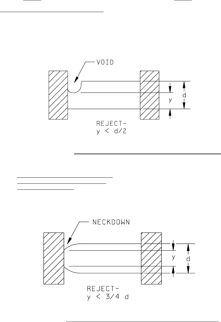
a. Voids at the terminal that reduces the a. Same as Class H
resistor width to less than 50 percent of
the original resistor width (see figure
2032-13h).
FIGURE 2032-13h. Class H film resistor width reduction at terminal by voids criterion
.
b. Neckdown at the terminal that reduces the
b. Same as Class H.
resistor width to less than 75 percent of
the original resistor width
(see figure
2032-14h).
FIGURE 2032-14h. Class H film resistor width reduction at terminal by necking criterion
.
MIL-STD-883F
METHOD 2032.2
18 June 2004
23
Class H Class K
3.1.6 c. Any sharp (clearly defined) color change 3.1.6 c. Same as class H.
within 0.1 mil of the terminal.
NOTE: A sharp color change close to the
terminal usually indicates an abrupt
reduction of resistor film thickness.
This color change usually occurs in a
straight line parallel to the terminal.
A gradual color change, or a nonuniform
or mottled color anywhere in the resistor,
is not cause for rejection.
d. Any resistor film lifting, peeling or d. Same as class H.
blistering.
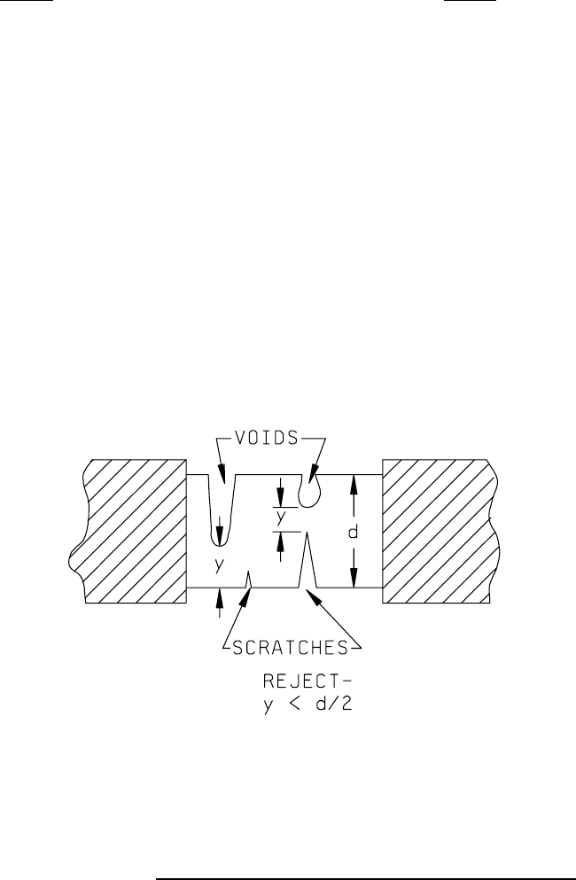
e. Reduction of resistor width, resulting from e. Same as class H.
voids, scratches, or a laser trim kerf or a
combination of these, that leaves less than
50 percent of the narrowest resistor width
(see figure 2032-15h).
PRECAUTIONARY NOTE: The maximum allowable
current density requirement shall not be exceeded.
FIGURE 2032-15h. Class H resistor width reduction by voids and scratches criteria
.