MIL- STD-883F 2004 TEST METHOD STANDARD MICROCIRCUITS.pdf - 第441页
MIL-STD-883F METHOD 2032.2 18 June 2004 35 C lass H Cla ss K 3.1. 7 h. A ker f in a res is tor, at the int erfac e 3.1.7 h. Same as cl ass H. of the r esis tor mater ial wi th the metalliz ation, th at leav es less t han…
MIL-STD-883F
METHOD 2032.2
18 June 2004
34
Class H Class K
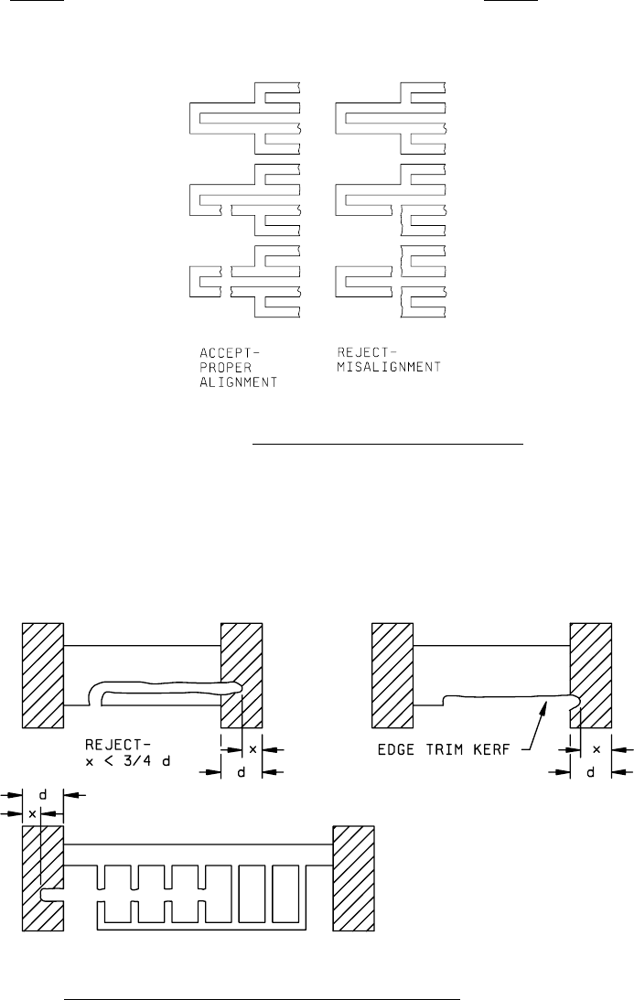
3.1.7 f. Kerf or scorch misalignment (see figure 3.1.7 f. Same as class H.
2032-31h).
FIGURE 2032-31h. Class H laser trim misalignment criteria
.
g. A kerf which extends into metallization and g. Same as class H.
leaves less than 75 percent of the
metallization width undisturbed (see figure
2032-32h).
NOTE: Opening a metallization link by design
is acceptable.
FIGURE 2032-32h. Class H laser trim kerf extension into metallization criteria
.
MIL-STD-883F
METHOD 2032.2
18 June 2004
35
Class H Class K
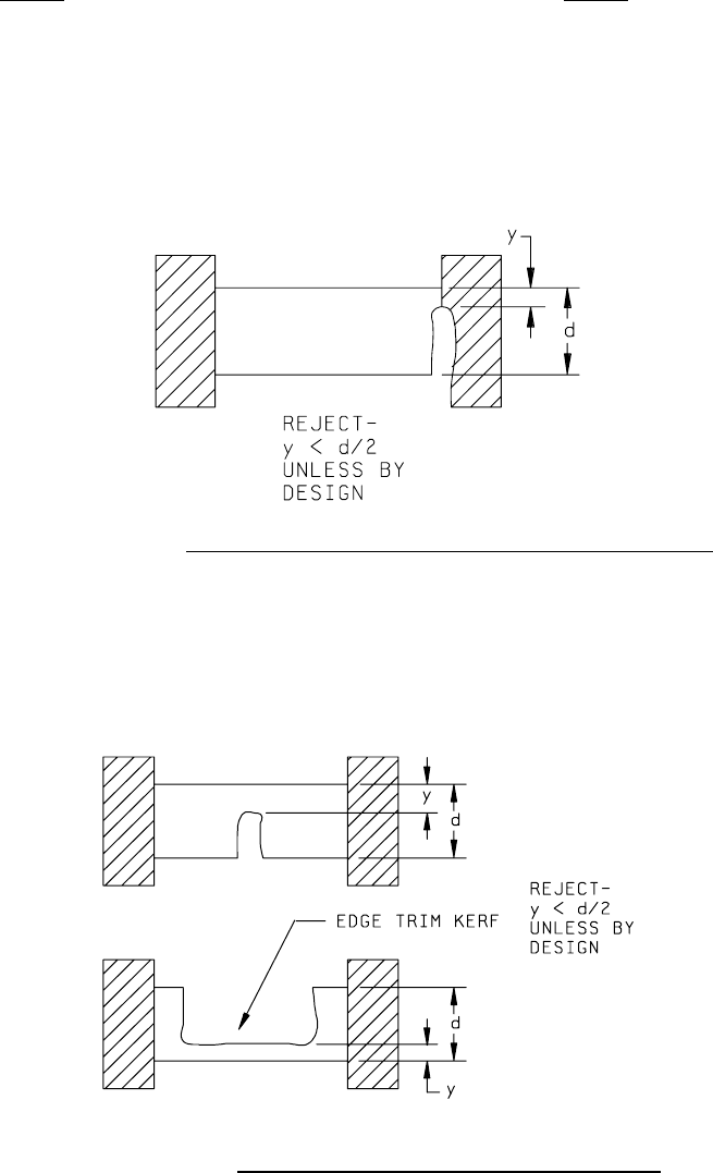
3.1.7 h. A kerf in a resistor, at the interface 3.1.7 h. Same as class H.
of the resistor material with the
metallization, that leaves less than 50 percent
of the original resistor width, unless by
design.
PRECAUTIONARY NOTE: The maximum
allowable current density requirement shall
not be exceeded. (see figure 2032-33h).
FIGURE 2032-33h. Class H resistor width reduction at metallization interface criteria
.
i. A kerf in a resistor that leaves less i. Same as class H.
than 50 percent of the original resistor width,
unless by design.
PRECAUTIONARY NOTE: The maximum allowable
current density requirement shall not be exceeded
(see figure 2032-34h).
FIGURE 2032-34h. Class H resistor width reduction by trimming criteria
.
MIL-STD-883F
METHOD 2032.2
18 June 2004
36
Class H Class K
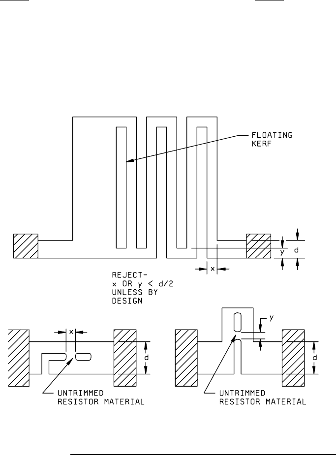
3.1.7 j. A kerf in a resistor that leaves less 3.1.7 j. Same as class H.
than 50 percent of the narrowest resistor
width unless by design (see figure 2032-35h).
NOTE: A floating kerf (one that is completely
contained within the resistor) must meet this
criteria.
PRECAUTIONARY NOTE: The maximum
allowable current density requirement shall
not be exceeded.
FIGURE 2032-35h. Class H resistor width reduction and untrimmed resistor material criteria
.
k. Pits into the silicon dioxide of conductive k. Same as class H.
substrate elements in the kerf which does
not show a line of separation between the
pit and the resistor material (see figure
2032-36h).