MIL- STD-883F 2004 TEST METHOD STANDARD MICROCIRCUITS.pdf - 第447页
MIL-STD-883F METHOD 2032.2 18 June 2004 41 Cla ss H Class K 3.2. 1.1 b. Scr atc h in the bonding pad ar ea that 3.2. 1.1 b. Less than 75 perc ent both exposes under lying mat erial and r educes (see figur e 2032-39k) . t…
MIL-STD-883F
METHOD 2032.2
18 June 2004
40
3.2 Planar thick film element inspection. Inspection for visual defects described in this section shall be
conducted on each planar thick film passive element. All inspection shall be performed at "low
magnification" within the range of 10X to 60X magnification for both class H and class K.
Class H
Class K
3.2.1 Operating metallization defects "low
magnification"
. No element shall be acceptable
that exhibits:
NOTE: The metallization defect criteria
contained in this section apply to operating
metallization only.
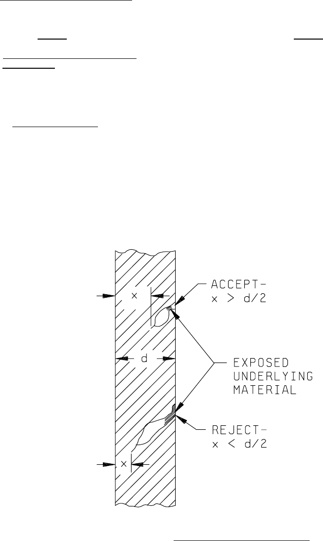
3.2.1.1 Metallization scratches
a. A scratch or probe mark in the metallization, a. Same as Class H.
excluding bonding pads, that both exposes
underlying material anywhere along its
length and leaves less than 50 percent of
the original metallization width undisturbed
(see figure 2032-38h).
NOTE: Underlying material does not have to be
exposed along the full length of the scratch.
NOTE: This criteria does not apply to
capacitors.
FIGURE 2032-38h. Class H metallization scratch criteria
.
MIL-STD-883F
METHOD 2032.2
18 June 2004
41
Class H Class K
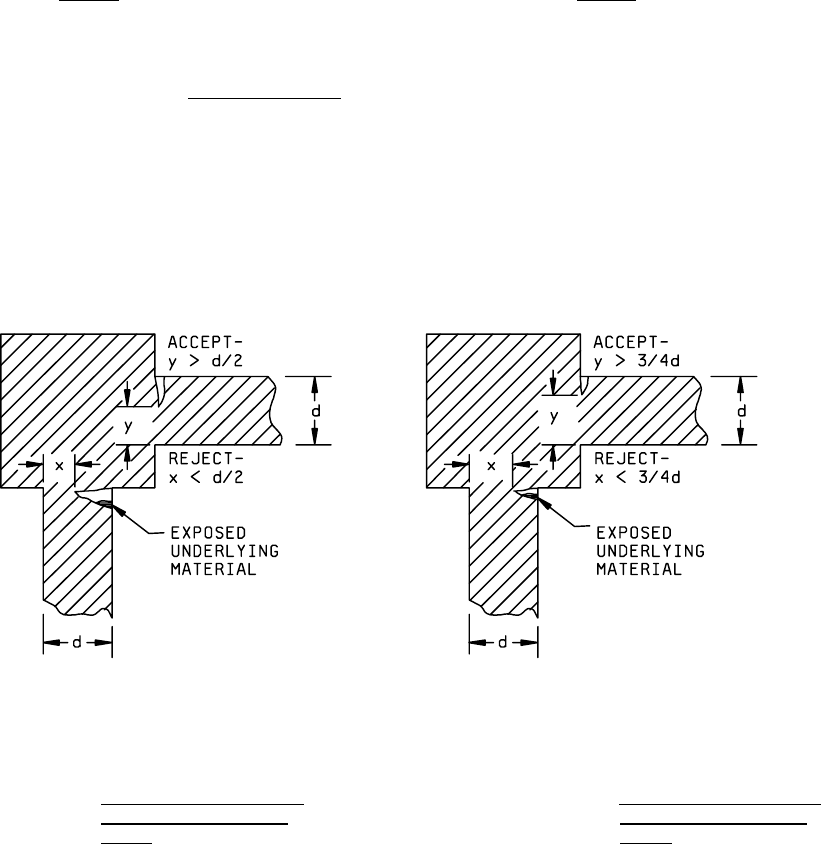
3.2.1.1 b. Scratch in the bonding pad area that 3.2.1.1 b. Less than 75 percent
both exposes underlying material and reduces (see figure 2032-39k).
the metallization path width, where it enters
the bonding pad, to less than 50 percent
its original metallization width. If two or
more metallization paths enter a bonding pad,
each shall be considered separately (see figure
2032-39h).
FIGURE 2032-39h. Class H metallization width
FIGURE 2032-39k. Class K metallization width
reduction at bonding pad
reduction at bonding pad
criteria
. criteria.
c. Scratch or probe marks in the bonding pad c. Same as class H
area that expose underlying material over
more than 25 percent of the original
metallization area.
MIL-STD-883F
METHOD 2032.2
18 June 2004
42
Class H Class K
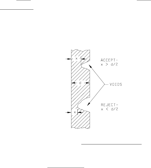
3.2.1.2 Metallization voids
.
a. Void(s) in the metallization, excluding a. Same as Class H.
bonding pads, that leaves less than 50 percent
of the original metallization width
undisturbed (see figure 2032-40h).
FIGURE 2032-40h. Class H metallization void criteria
.
b. Void(s) in the bonding pad area that reduces b. Less than 75 percent.
the metallization path width, where it enters
the bonding pad, to less than 50 percent
of
its original metallization width. If two or
more metallization paths enter a bonding pad,
each shall be considered separately.
NOTE: Figures 2032-39h and 2032-39k
illustrate metallization width reduction at
bonding pad criteria for scratches. Void
criteria are similar.
c. Void(s) in the bonding pad area that expose c. Same as class H.
underlying material over more than 25 percent
of the original metallization area.
NOTE: For RF microwave elements on nonconductive
substrates, a void created in the bonding pad
area as a result of wire bond removal for
performance optimization or tuning, is not
rejectable provided that the void remains
entirely visible.