MIL- STD-883F 2004 TEST METHOD STANDARD MICROCIRCUITS.pdf - 第461页
MIL-STD-883F METHOD 2032.2 18 June 2004 55 Class H Class K 3.2.4 d. A k erf t hat leaves less than 50 perc ent 3.2. 4 d. Same as c lass H. of the or iginal wi dth of a r esis tor, unless by design ( see f igure 2032-52Ah…
MIL-STD-883F
METHOD 2032.2
18 June 2004
54
Class H Class K
3.2.4 Trimmed thick film resistor defects, "low
magnification"
. No element shall be acceptable that
exhibits:
NOTE: The trim defect criteria contained in this
section apply to active resistor areas only.
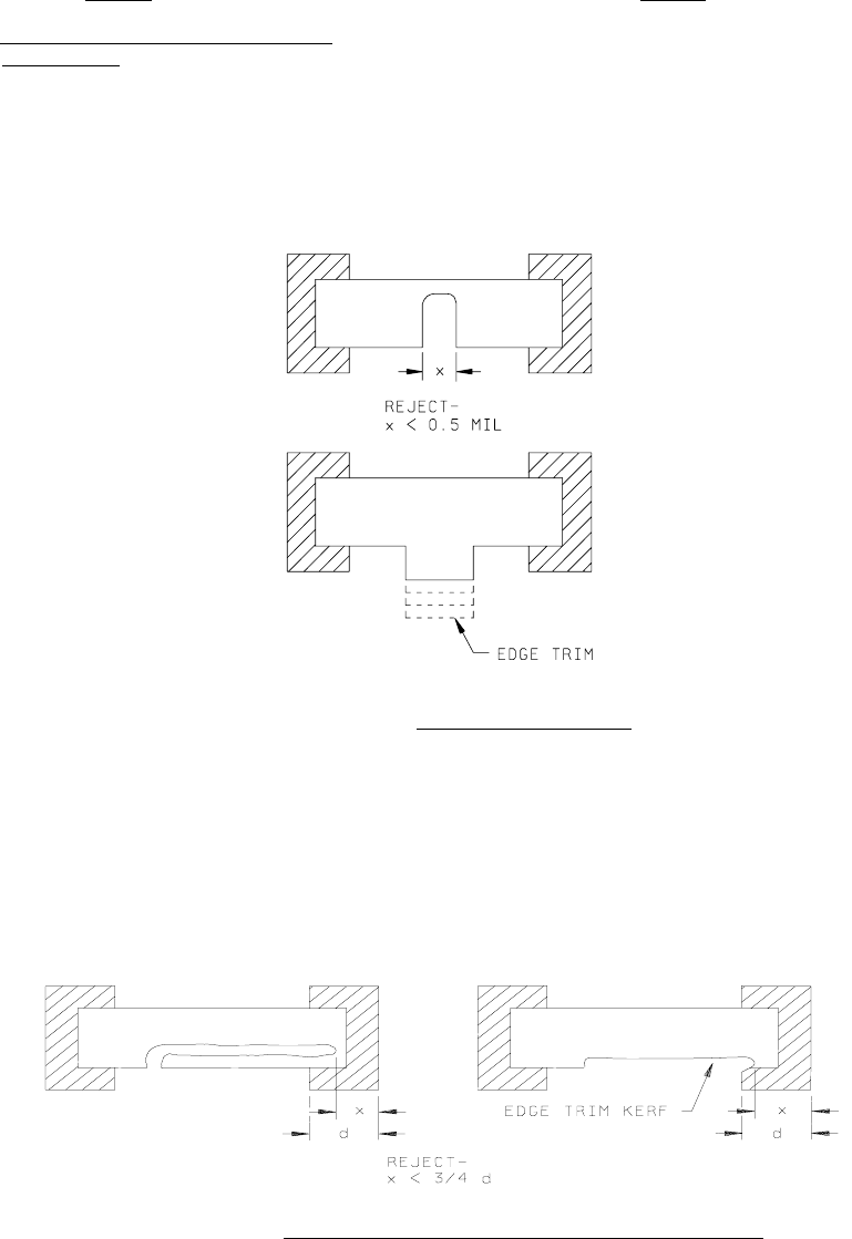
a. A kerf width less than 0.5 mil (see figure a. Same as class H.
2032-51h).
NOTE: This does not apply to edge trimming.
FIGURE 2032-51h. Class H kerf width criteria
.
b. A kerf containing detritus. b. Same as class H.
c. A kerf which extends into metallization c. Same as class H.
and leave less than 75 percent of
the metallization width undisturbed
(see figure 2032-52h).
NOTE: Opening a metallization link by
design is acceptable.
FIGURE 2032-52h. Class H laser trim kerf extension into metallization criteria
.
MIL-STD-883F
METHOD 2032.2
18 June 2004
55
Class H Class K
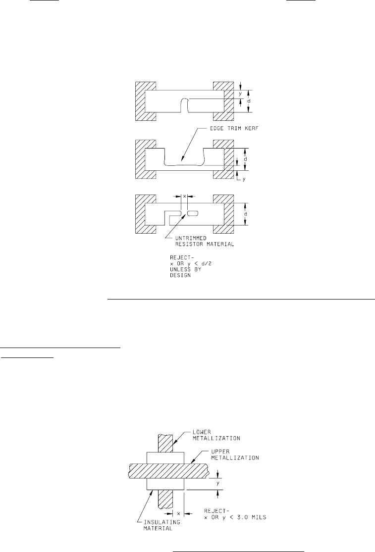
3.2.4 d. A kerf that leaves less than 50 percent 3.2.4 d. Same as class H.
of the original width of a resistor,
unless by design (see figure 2032-52Ah).
PRECAUTIONARY NOTE: The maximum allowable
current density requirement shall not be exceeded.
FIGURE 2032-52Ah. Class H resistor width reduction and untrimmed resistor material criteria
.
e. A trim that does not originate from the edge e. Same as class H.
of the resistor.
3.2.5 Multilevel thick film defects, "low
magnification"
. No element shall be acceptable
that exhibits:
a. Any insulating material that does not a. Same as class H.
extend beyond the width of the upper and
lower metallization by 3.0 mils minimum
(see figure 2032-53h).
FIGURE 2032-53h. Class H dielectric extension criteria
.
MIL-STD-883F
METHOD 2032.2
18 June 2004
56
Class H Class K
3.2.5 b. Voids in the insulating material 3.2.5 b. Same as class H.
that expose underlying metallization.
c. Vias that are less than 50 percent of the c. Same as class H.
original design area.
d. Scratch that completely crosses the d. Same as class H.
metallization and damages the
insulating material surface on either
side.
3.2.6 All thick film capacitors and those overlay capacitors used in GaAs microwave devices,"low
magnification"
. No element shall be acceptable that exhibits:
a. Scratches that expose an underlying material.
b. Any peeling or lifting of the metallization.
c. Excess top metal which extend beyond the capacitor bottom metal.
d. Voids in the capacitor bottom metal which extend under the capacitor top metal.
e. Voids in the top metallization which leaves less than 75% of the metallization area undisturbed.
3.3 Nonplanar element inspection
. Inspection for visual defects described in this section shall be conducted on each
nonplanar passive element. The "low magnification" inspection shall be within the range of 10X to 60X.
Class H
Class K
3.3.1 General nonplanar element defects,
"low magnification"
. No element shall be acceptable that exhibits:
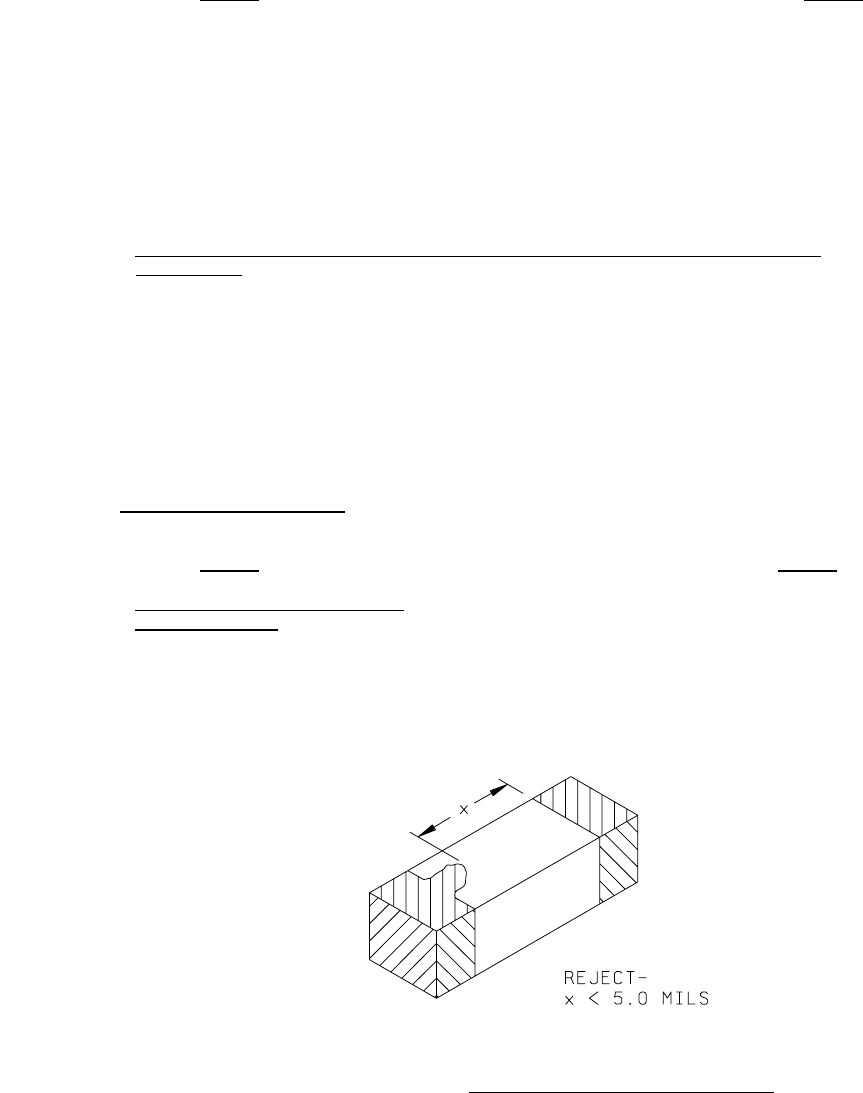
a. Peeling or lifting of any metallization. a. Same as class H.
b. Protrusion between metallization terminals b. Same as class H.
that leaves less than 5.0 mils separation
(see figure 2032-54h).
FIGURE 2032-54h. Class H metallization protrusion criterion
.
*