MIL- STD-883F 2004 TEST METHOD STANDARD MICROCIRCUITS.pdf - 第467页
MIL-STD-883F METHOD 2032.2 18 June 2004 61 Cla ss H Class K 3.3.4 e. Metallized terminal n ot ali gned as shown in 3.3.4 e. Same as clas s H. the appli cable dr awing. f. Enc apsulant preventi ng the metall ized f . Same…
MIL-STD-883F
METHOD 2032.2
18 June 2004
60
Class H Class K
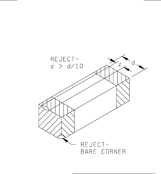
3.3.3 e. Void in the metallized edges of the 3.3.3 e. Same as class H.
element that are greater than 10 percent
of the metallized edge dimension, or bare
corners of metallized terminals
(see figure 2032-59h).
NOTE: This criteria ia applicable to
solder attached elements only.
FIGURE 2032-59h. Class H metallized edge defect criteria
.
f. Attached foreign material on the body that f. Same as class H.
covers an area greater than 5.0 mils
square on any side.
3.3.4 Tantalum chip capacitor defects, "low
magnification." No element shall be acceptable that
exhibits:
a. Flaking or peeling of the encapsulant that a. Same as class H.
exposes any underlying material.
b. A metallized terminal that is less than 90 b. Same as class H.
percent free of encapsulant material.
c. Less than 50 percent continuous metallized c. Same as class H.
terminal weld area without cracks. For capacitors
with riser wires, a riser wire connection with less
than 25 percent continuous weld area.
d. Metallized terminal containing residue from the d. Same as class H.
welding operation that is not firmly
attached metallurgically to the anode cap.
MIL-STD-883F
METHOD 2032.2
18 June 2004
61
Class H Class K
3.3.4 e. Metallized terminal not aligned as shown in 3.3.4 e. Same as class H.
the applicable drawing.
f. Encapsulant preventing the metallized f. Same as class H.
terminal from resting on the substrate
bonding pads when the capacitor is in
the bonding position except where the
metallized terminal electrical contact
is made by alternate means.
g. Lifting, blistering or peeling of metallized g. Same as class H.
terminal encapsulant.
3.3.5 Parallel plate chip capacitor defects,
"low magnification"
. No element shall be acceptable
that exhibits:
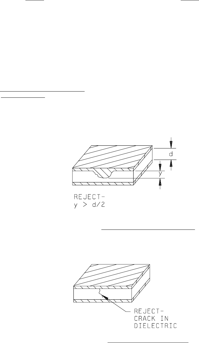
a. Metallization that extends greater than 50 a. Same as class H.
percent around the edge of the capacitor
(see figure 2032-60h).
FIGURE 2032-60h. Class H metallization extension criterion
.
3.3.5 b. Evidence of cracks in the dielectric body 3.3.5 b. Same as class H.
(see figure 2032-61h).
FIGURE 2032-61h. Class H crack in dielectric criterion
.
MIL-STD-883F
METHOD 2032.2
18 June 2004
62
3.3.6 Inductor and transformer defects, "low
magnification"
. No element shall be acceptable
that exhibits:
a. Peeling, lifting or blistering of winding a. Same as class H.
metallization or insulation.
b. Evidence of shorts between adjacent turns or b. Same as class H.
windings.
c. Cracks or exposure of bare magnetic core c. Same as class H.
material. Exposed bare magnetic core material
is acceptable if by design.
d. Pits or voids in the core insulation greater d. Same as class H.
than 5.0 mils area that expose the magnetic
core material.
e. Separation less than 5.0 mils between wire e. Same as class H.
termination points of the same or adjacent
windings.
f. Missing polarity identification unless by f. Same as class H.
design.
g. Operating metallization and multilevel thick g. Same as class H.
film defects as described in 3.2.1 and
3.2.5 herein.
3.3.7 Chip resistor defects, "low magnification"
.
No element shall be acceptable that exhibits:
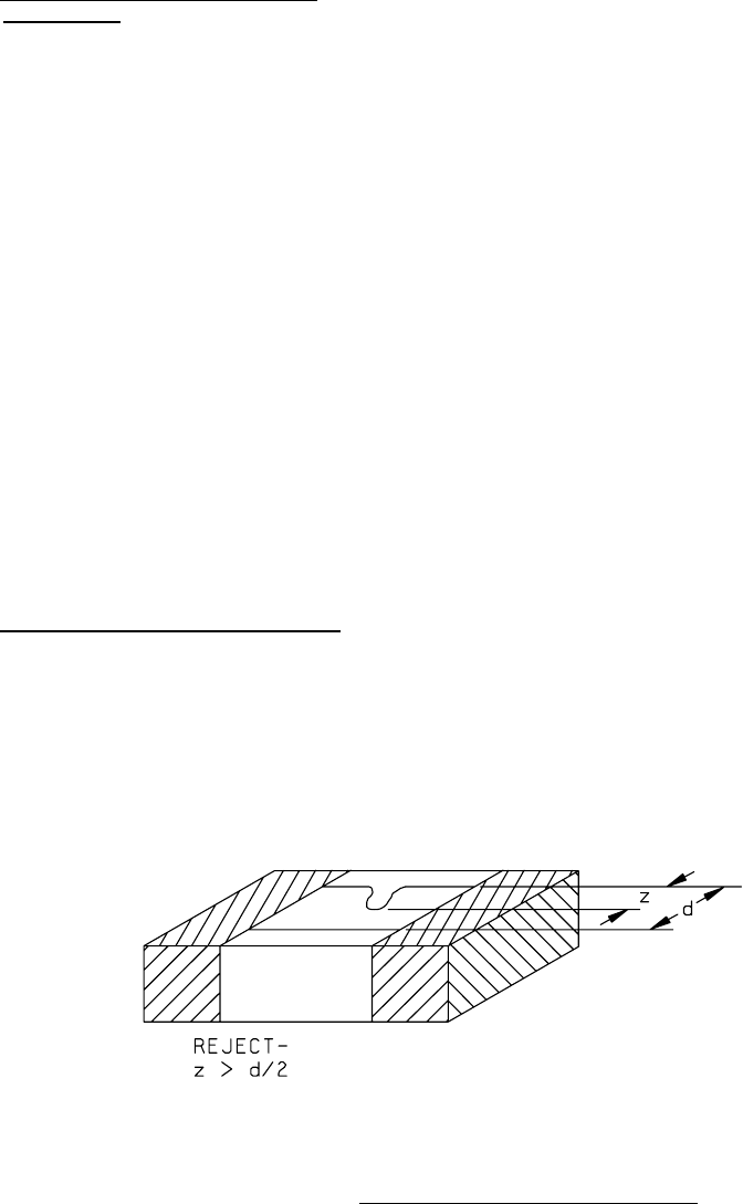
a. Reduction of the resistor width resulting from a. Same as class H.
voids, bubbles, nicks, or scratches, or a
combination of these, that leaves less than 50
percent of the narrowest resistor width (see
figure 2032-62h).
FIGURE 2032-62h. Class H resistor width reduction criterion
.