MIL- STD-883F 2004 TEST METHOD STANDARD MICROCIRCUITS.pdf - 第480页
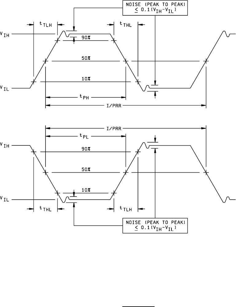
MIL-STD-883F METHOD 3001.1 15 November 1974 2 FI GURE 3001-1. Dr ive sour ces .

MIL-STD-883F
METHOD 3001.1
15 November 1974
1
METHOD 3001.1
DRIVE SOURCE, DYNAMIC
1. PURPOSE
. This method establishes a drive source to be used in measuring dynamic performance of digital
microelectronic devices, such as TTL, DTL, RTL, ECL, and MOS.
2. APPARATUS
. The drive source shall supply a smooth transition between specified voltage levels. The signal
characteristics shall not vary outside of their prescribed tolerances when interfaced with the device under test (device in the
test socket).
3. PROCEDURE
. The drive source shall be measured at the input terminal of the test socket (no device in the test
socket). Figure 3001-1 shows typical driving source waveforms and should be used specifying the parameters shown,
unless otherwise stated in the applicable acquisition document.
3.1 Pulse amplitude
. The specified HIGH level of the driving source shall be greater than the V
OH
of the device. The
specified LOW level of the driving source shall be less than V
OL
of the device.
3.2 Transition times
. The transition times of the driving source (t
THL
and t
TLH
) shall be faster than the transition time of the
device being tested, unless otherwise stated in the acquisition document. The transition times shall normally be measured
between the 10 percent and 90 percent levels of the specified pulse.
3.3 Pulse repetition rate (PRR)
. Unless the pulse repetition rate is the parameter being tested, it shall be chosen so that
doubling the rate or reducing by a half will not affect the measurement results.
3.4 Duty factors (duty cycles)
. The duty cycles of the driving source shall be chosen so that a 10 percent variation in the
duty cycle will not affect the measurement results. The duty cycle shall be defined with respect to either a positive or
negative pulse. The pulse width (t
p
) of the input pulses shall be measured between the specified input measurement levels.
When more than one pulse input is needed to test a device, the duty cycle of the prime input (i.e., clock, etc.) shall be
specified. The phase relationship of all other input pulses shall be referenced to the prime input pulse.
4. SUMMARY
. The following details, when applicable, shall be specified in the applicable acquisition document:
a. Levels V
IL
and V
IH
.
b. Driving signal transition times.
c. Pulse repetition rate.
d. Duty factors.
e. Recommended pulse generator, if required.
f. Input measurement levels, if other than those shown in figure 3001-1.
MIL-STD-883F
METHOD 3001.1
15 November 1974
2
FIGURE 3001-1. Drive sources
.

MIL-STD-883F
METHOD 3002.1
15 November 1974
1
METHOD 3002.1
LOAD CONDITIONS
1. PURPOSE
. This method establishes the load conditions to be used in measuring the static and dynamic performance
of digital microelectronic devices such as TTL, DTL, RTL, ECL, and MOS.
2. APPARATUS
. The load for static tests shall simulate the worst case conditions for the circuit parameters being tested.
The load for dynamic tests shall simulate a specified use condition for the parameters being tested. The loads shall be
specified in the applicable acquisition document.
2.1 Discrete component load
. The load will consist of any combination of capacitive, inductive, resistive, or diode
components.
2.1.1 Capacitive load (C
L
). The total load capacitance of the circuit under test shall include probe and test fixture
capacitance and a compensating capacitor as required. The value of the capacitance, measured at 1 MHz ±10 percent,
shall be specified in the applicable acquisition document.
2.1.2 Inductive load (L
L
). The total load inductance of the circuit under test shall include probe and test fixture inductance
and a compensating inductor as required. The value of the inductance, measured at 1 MHz ±10 percent, shall be specified
in the applicable acquisition document.
2.1.3 Resistive load (R
L
). The resistive load shall represent the worst case fan out conditions of the device under test for
static tests and a specified fan out condition for dynamic tests. For sink loads, the resistor shall be connected between the
power supply (V
CC
or V
DD
) and the circuit output for TTL, DTL, RTL, C-MOS, and MOS (N-Channel) and between circuit
output and ground for MOS (P-Channel). For source loads, the resistor shall be connected between circuit output and
ground for TTL, DTL, RTL, C-MOS, and MOS (N-Channel) and between V
DD
and the circuit output for MOS (P-Channel).
For ECL devices, the load resistors are connected from the output to a specified negative voltage.
2.1.4 Diode load (D
L
). The diode load shall represent the input diode(s) of the circuit under test. The equivalent diode, as
specified in the applicable acquisition document, will also represent the base-emitter or base-collector diode of any transistor
in the circuit path of the normal load.
2.2 Dynamic load change
. The load shall automatically change its electrical parameters as the device under test changes
logic state if this is the normal situation for the particular family of circuits being tested. One method of accomplishing this
dynamic change is to simulate devices or use actual devices from the same logic family equal to the specified load.
3. PROCEDURE
. The load will normally be paralleled by a high impedance voltage detection indicator. The indicator
may be either visual or memory storage.
4. SUMMARY
. The following shall be defined in the applicable acquisition document:
a. Capacitive load (see 2.1.1).
b. Inductive load (see 2.1.2).
c. Resistive load (see 2.1.3).
d. Diode load, the 1NXXX number and any associated critical parameters shall be specified (see 2.1.4).
e. Negative voltage, when using a resistive load for ECL (see 2.1.3).