MIL- STD-883F 2004 TEST METHOD STANDARD MICROCIRCUITS.pdf - 第481页
MIL-STD-883F METHOD 3002.1 15 November 1974 1 METHOD 3002.1 LOAD CONDITIONS 1. PURPOSE . This method est ablis hes the l oad condit ions t o be used in meas uring t he stat ic and dynami c perf ormanc e of digit al mic r…
MIL-STD-883F
METHOD 3001.1
15 November 1974
2
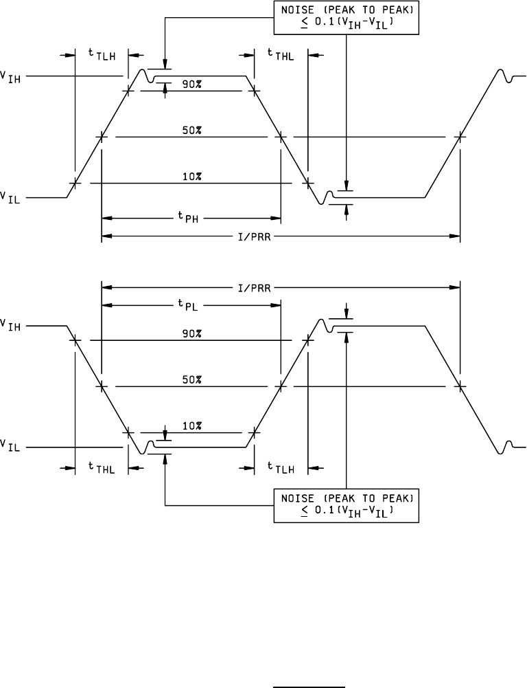
FIGURE 3001-1. Drive sources
.

MIL-STD-883F
METHOD 3002.1
15 November 1974
1
METHOD 3002.1
LOAD CONDITIONS
1. PURPOSE
. This method establishes the load conditions to be used in measuring the static and dynamic performance
of digital microelectronic devices such as TTL, DTL, RTL, ECL, and MOS.
2. APPARATUS
. The load for static tests shall simulate the worst case conditions for the circuit parameters being tested.
The load for dynamic tests shall simulate a specified use condition for the parameters being tested. The loads shall be
specified in the applicable acquisition document.
2.1 Discrete component load
. The load will consist of any combination of capacitive, inductive, resistive, or diode
components.
2.1.1 Capacitive load (C
L
). The total load capacitance of the circuit under test shall include probe and test fixture
capacitance and a compensating capacitor as required. The value of the capacitance, measured at 1 MHz ±10 percent,
shall be specified in the applicable acquisition document.
2.1.2 Inductive load (L
L
). The total load inductance of the circuit under test shall include probe and test fixture inductance
and a compensating inductor as required. The value of the inductance, measured at 1 MHz ±10 percent, shall be specified
in the applicable acquisition document.
2.1.3 Resistive load (R
L
). The resistive load shall represent the worst case fan out conditions of the device under test for
static tests and a specified fan out condition for dynamic tests. For sink loads, the resistor shall be connected between the
power supply (V
CC
or V
DD
) and the circuit output for TTL, DTL, RTL, C-MOS, and MOS (N-Channel) and between circuit
output and ground for MOS (P-Channel). For source loads, the resistor shall be connected between circuit output and
ground for TTL, DTL, RTL, C-MOS, and MOS (N-Channel) and between V
DD
and the circuit output for MOS (P-Channel).
For ECL devices, the load resistors are connected from the output to a specified negative voltage.
2.1.4 Diode load (D
L
). The diode load shall represent the input diode(s) of the circuit under test. The equivalent diode, as
specified in the applicable acquisition document, will also represent the base-emitter or base-collector diode of any transistor
in the circuit path of the normal load.
2.2 Dynamic load change
. The load shall automatically change its electrical parameters as the device under test changes
logic state if this is the normal situation for the particular family of circuits being tested. One method of accomplishing this
dynamic change is to simulate devices or use actual devices from the same logic family equal to the specified load.
3. PROCEDURE
. The load will normally be paralleled by a high impedance voltage detection indicator. The indicator
may be either visual or memory storage.
4. SUMMARY
. The following shall be defined in the applicable acquisition document:
a. Capacitive load (see 2.1.1).
b. Inductive load (see 2.1.2).
c. Resistive load (see 2.1.3).
d. Diode load, the 1NXXX number and any associated critical parameters shall be specified (see 2.1.4).
e. Negative voltage, when using a resistive load for ECL (see 2.1.3).
MIL-STD-883F
METHOD 3002.1
15 November 1974
2
This page intentionally left blank