MIL- STD-883F 2004 TEST METHOD STANDARD MICROCIRCUITS.pdf - 第489页
MIL-STD-883F METHOD 3005.1 15 November 1974 1 METHOD 3005.1 POW ER SUPPLY CURRENT 1. PURPOSE . This method est ablis hes the means for meas uring power supply c urrent s of di gital mi croel ectr onic devi ces such as TT…
MIL-STD-883F
METHOD 3004.1
15 November 1974
2
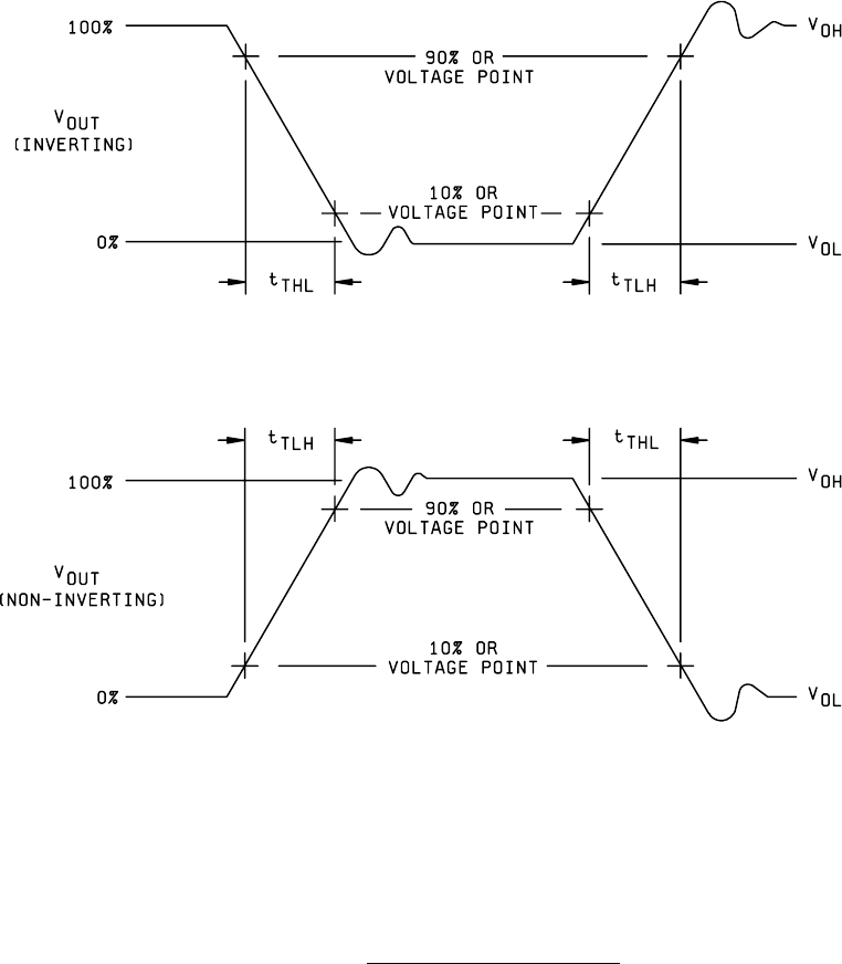
FIGURE 3004-1. Transition time measurements
.
MIL-STD-883F
METHOD 3005.1
15 November 1974
1
METHOD 3005.1
POWER SUPPLY CURRENT
1. PURPOSE
. This method establishes the means for measuring power supply currents of digital microelectronic devices
such as TTL, DTL, RTL, ECL, and MOS.
2. APPARATUS
. Equipment capable of applying prescribed voltage to the test circuit power supply terminals and
measuring the resultant currents flowing in these terminals shall be provided. The test chamber shall be capable of
maintaining the device under test at any specified temperature.
3. PROCEDURE
. The device shall be stabilized at the specified test temperature.
3.1 I
CCH
(logic gate). Inputs of the device under test shall be conditioned in such a way as to provide a HIGH level at the
output, the worst case supply voltage(s) shall be applied and the resultant current flow in the supply terminals measured.
3.2 I
CCL
(logic gate). Inputs of the device under test shall be conditioned in such a way as to provide a LOW level at the
output, the worst case supply voltages(s) shall be applied and the resultant current flow in the supply terminals measured.
3.3 I
CC
or I
EE
of combinatorial digital circuits. The inputs of the device under test shall be conditioned to put the device into
its worst case power dissipating state. The current flowing into the V
CC
, (positive supply) terminal, or out of the V
EE
(negative supply) terminal shall be measured with the V
CC
and V
EE
voltages at their maximum specified operating levels.
3.4 I
CC
or I
EE
of sequential digital circuits. The inputs of the device under test shall be exercised to put the device in a
known output state (either HIGH or LOW) that causes worst case power dissipation. The current flowing into the V
CC
(positive supply) terminal, or out of the V
EE
(negative supply) terminal shall be measured with the V
CC
and V
EE
voltages at
their maximum specified operating levels.
3.5 I
DD
(MOS logic gate). Inputs of the device under test shall be conditioned in such a way as to provide a HIGH level at
the output of MOS (P-Channel and C-MOS) or a LOW level at the output of MOS (N-Channel and C-MOS); worst case
voltage(s) shall be applied and the resultant current in the supply terminals measured.
3.6 I
GG
(MOS P-Channel and N-Channel logic gates). Inputs of the device under test shall be conditioned in such a way
as to provide a HIGH level at the output of MOS (P-Channel) or a LOW level at the output of MOS (N-Channel); worst case
voltage(s) shall be applied and the resultant current flow in the supply terminals measured.
3.7 I
DD
of MOS combinatorial circuits. See 3.3 above.
3.8 I
DD
of MOS sequential circuits. See 3.4 above.
3.9 I
GG
of MOS combinatorial circuits. See 3.3 above.
3.10 I
GG
of MOS sequential circuits. See 3.4 above.
3.11 I
DD
dynamic (MOS logic gating and flip flop circuits). The driving signal to the test circuit shall be provided according
to method 3001 of this standard; the worst case voltage(s) shall be applied and the resultant average current in the supply
terminals measured.

MIL-STD-883F
METHOD 3005.1
15 November 1974
2
4. SUMMARY. The following details shall be specified in the applicable acquisition document:
a. Test temperature.
b. Power supply voltages.
c. I
CCH
, I
CCL,
I
DD
, I
GG
, and I
EE
limits.
d. Conditioning voltages.
e. Dynamic input parameters (see 3.11).