MIL- STD-883F 2004 TEST METHOD STANDARD MICROCIRCUITS.pdf - 第508页
MIL-STD-883F METHOD 3013.1 15 November 1974 4 4. SUMMARY . The followi ng details , when appli cable, shall be speci fied i n the appli cable ac quisi tion doc ument: a. V IL (max ). b. V IL (min). c. V IH (min). d. V IH…
MIL-STD-883F
METHOD 3013.1
15 November 1974
3
3.2 Test procedure for dc noise margin.
3.2.1 Worse case configuration
. The measurement of dc noise margin using a particular logic input terminal should
correspond to the worst case test configuration in the applicable acquisition document. For example, the measurement of
LOW level noise margin for a positive-logic inverting NAND gate should be performed under the same worst case test
conditions as the dc measurement of V
OH
(min). If the worst case dc test conditions for V
OH
(min) are high power supply
voltage, all unused logic inputs connected to V
OH
(min) and output current equal to zero, these conditions should be applied
to the corresponding dc noise margin measurement.
3.2.2 LOW level noise margin, V
NL
. The LOW level noise margin test is normally performed during the V
OH
test for
inverting logic and during the V
OL
test for noninverting logic. The noise margin is calculated from the following expression:
V
NL
= V
IL
(max) - V
OL
(max)
3.2.3 HIGH level noise margin, V
NH
. The HIGH level noise margin test is performed during the V
OL
test for inverting logic
and during the V
OH
test for noninverting logic. The noise margin is calculated from the following expression:
V
NH
= V
OH
(min) - V
IH
(min)
3.2.4 Negative ground noise margin, V
NG
. With all power supply and output terminals connected to the appropriate worst
case conditions, apply V
OL
(max) to the inputs specified in the applicable acquisition document and decrease the voltage
applied to the ground terminal until the output levels equal V
IH
(min) for inverting logic and V
IL
(max) for noninverting logic.
The dc ground noise margin is the voltage measured at the device ground terminal. The dc source resistance of the injected
ground line voltage shall be negligible.
3.2.5 Positive ground noise margin, V
NG+
. With all power supply and output terminals connected to the appropriate worst
case conditions, apply V
OH
(min) to the inputs specified in the applicable acquisition document and increase the voltage
applied to the ground terminal until the output levels equal V
IL
(max) for inverting logic and V
IH
(min) for noninverting logic.
The dc ground noise margin is the voltage measured at the device ground terminal. The dc source resistance of the injected
ground line voltage shall be negligible.
3.2.6 Power supply noise margin, V
NP+
or V
NP-
. With all input, power supply, and output terminals connected to the
appropriate worst case conditions, increase (or decrease) the power supply voltage(s) until the output level equals the
appropriate logic level limit. The power supply noise margin is the difference between the measured supply voltage(s) and
the appropriate noise-free worst case supply voltage level(s). If more than one power supply is required, the noise margin of
each supply should be measured separately.
3.3 Test procedure for ac noise margin
.
3.3.1 AC noise margin test point
. If, for any combination of noise pulse width or transition times, the ac noise margin is
less than the dc noise margin, the noise pulse amplitude, pulse width, and transition time which produce the minimum noise
margin shall be used as the conditions for test. If the ac noise margin exceeds the dc noise margin, the dc noise margin
tests only shall be performed.
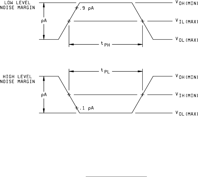
3.3.2 LOW level noise margin, pulse width, T
PL
. With all unused logic input, power supply, and output terminals
connected to the appropriate worst case conditions, a positive-going noise pulse shall be applied to the input under test.
The pulse amplitude shall be equal to V
OH
(min) minus V
OL
(max); the pulse amplitude shall be equal to V
OH
(max); and the
transition times shall be much less than the minimum transition times of the device under test. The test is performed by
initially adjusting the input pulse width at the 0.9 amplitude level to one and one quarter times the rise time. The pulse width
is increased until the output voltage is equal to V
IH
(max) for inverting logic and equal to V
IL
(min) for noninverting logic. The
noise margin pulse width is then measured at the input pulse V
IL
(max) level.
3.3.3 HIGH level noise margin, pulse width, T
PH
. With all unused logic input, power supply, and output terminals
connected to the appropriate worst case conditions, a negative-going noise pulse shall be applied to the input under test.
The pulse amplitude shall be equal to V
OH
(min) minus V
OL
(max); the pulse shall be superimposed on a dc level equal to
V
OH
(min); and the transition times shall be much less than the minimum transition times of the device under test. The test is
performed by initially adjusting the input pulse width at the 0.1 amplitude level to one and one quarter times the rise time.
The pulse width is increased until the output voltage is equal to V
IL
(min) for inverting logic and V
IH
(max) for noninverting
logic. The noise margin pulse width is then measured at the input pulse V
IH
(min) level.

MIL-STD-883F
METHOD 3013.1
15 November 1974
4
4. SUMMARY. The following details, when applicable, shall be specified in the applicable acquisition document:
a. V
IL
(max).
b. V
IL
(min).
c. V
IH
(min).
d. V
IH
(max).
e. V
OL
(max).
f. V
OH
(min).
g. V
NL
.
h. V
NH
.
i. V
NG
.
j. V
NP
.
k. t
PL
.
l. t
PH
.
m. Test temperature. Unless otherwise specified, dc noise margin measurements shall be made at the rated
operating temperature extremes in addition to any other nominal test temperatures.
n. Specific noise margin measurements and conditions which are to be performed.
o. Power supply voltages.
p. Input conditioning voltages.
q. Output loads.
r. Parameters of noise signal.
MIL-STD-883F
METHOD 3013.1
15 November 1974
5
FIGURE 3013-1. Definitions of noise pulse width
.