MIL- STD-883F 2004 TEST METHOD STANDARD MICROCIRCUITS.pdf - 第517页
MIL-STD-883F METHOD 3015.7 22 March 1989 3 b. A new sampl e of devices shall be s elected and s ubjected t o the next lower voltage step us ed. Eac h device shal l be tested using three pos itive and three negativ e puls…
MIL-STD-883F
METHOD 3015.7
22 March 1989
2
3.1.2 Test temperature. Each device shall be stabilized at room temperature prior to and during testing.
3.1.3 ESD classification testing
. ESD classification testing of devices shall be considered destructive.
3.2 ESD simulator current waveform verification
. To ensure proper simulator operation, the current waveform verification
procedure shall be done, as a minimum, at the beginning of each shift when ESD testing is performed, or prior to testing
after each change of the socket/board, whichever is sooner. If the simulator does not meet all requirements, all
classification testing done since the last successful verification shall be repeated. At the time of initial facility certification
and recertifications, photographs shall be taken of the waveforms observed as required by 3.2c through 3.2e and be kept on
file for purposes of audit and comparison. (Stored digitized representations of the waveforms are acceptable in place of
photographs.)
a. With the DUT socket installed on the simulator, and with no DUT in the socket, place a short (figure 3015-1)
across two pins of the DUT socket and connect one of the pins to simulator terminal A and the other pin to terminal
B.
b. Connect the current probe around the short near terminal B (see figure 3015-1). Set the simulator charging
voltage source V
S
to 4,000 volts corresponding to step 4 of table I.
c. Initiate a simulator pulse and observe the leading edge of the current waveform. The current waveform shall meet
the rise time, peak current, and ringing requirements of figure 3015-2.
d. Initiate a simulator pulse again and observe the complete current waveform. The pulse shall meet the decay time
and ringing requirement of figure 3015-2.
e. Repeat the above verification procedure using the opposite polarity
(V
S
= -4,000 volts).
f. It is recommended that the simulator output be checked to verify that there is only one pulse per initiation, and that
there is no pulse while capacitor C1 is being charged. To observe the recharge transient, set the trigger to the
opposite polarity, increase the vertical sensitivity by approximately a factor of 10, and initiate a pulse.
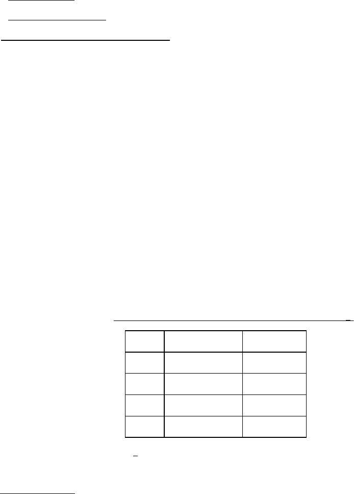
TABLE I. Simulator charging voltage (V
S
) steps versus peak current (I
P
). 1/
Step
V
S
(volts) I
P
(amperes)
1 500 0.33
2 1,000 0.67
3 2,000 1.33
4 4,000 2.67
1
/ I
P
is the current flowing through R2 during
the current waveform verification procedure
and which is approximately V
S
/1,500 ohms.
3.3 Classification testing
.
a. A sample of devices (see 4.c) shall be characterized for the device ESD failure threshold using the voltage steps shown
in table I, as a minimum. Finer voltage steps may optionally be used to obtain a more accurate measure of the failure
voltage. Testing may begin at any voltage step, except for devices which have demonstrated healing effects, including
those with spark gap protection, which shall be started at the lowest step. Examination of known technology family input
or output V/I damage characteristics (i.e., curve tracer), or other simplified test verification techniques may be used to
validate the failure threshold (e.g., cumulative damage effects may be eliminated by retesting at the failure voltage step
using a new sample of devices and possibly passing the step).
MIL-STD-883F
METHOD 3015.7
22 March 1989
3
b. A new sample of devices shall be selected and subjected to the next lower voltage step used. Each device shall be
tested using three positive and three negative pulses using each of the pin combinations shown in table II. A minimum
of 1 second delay shall separate the pulses.
c. The sample devices shall be electrically tested to subgroups 1 and 7 as applicable (room temperature dc parameters and
functional tests).
d. If one or more of the devices fail, the testing of 3.3b and 3.3c shall be repeated at the next lower voltage step used.
e. If none of the devices fail, record the failure threshold determined in 3.3a. Note the highest step passed, and use it to
classify the device according to table III.
TABLE II. Pin combinations to be tested
. 1/ 2/
Terminal A
(Each pin individually
connected to terminal A
with the other floating)
Terminal B
(The common combination
of all like-named pins
connected to terminal B)
1. All pins except V
ps1
3/ All V
ps1
pins
2. All input and output pins All other input-output pins
1
/ Table II is restated in narrative form in 3.4 below.
2
/ No connects are not to be tested.
3
/ Repeat pin combination 1 for each named power supply and for ground (e.g.,
where V
ps1
is V
DD
, V
CC
, V
SS
, V
BB
, GND, +V
S
, -V
S
, V
REF
, etc.)
3.4 Pin combination to be tested
.
a. Each pin individually connected to terminal A with respect to the device ground pin(s) connected to terminal B. All pins
except the one being tested and the ground pin(s) shall be open.
b. Each pin individually connected to terminal A with respect to each different set of a combination of all named power
supply pins (e.g., V
SS1
or V
SS2
or V
SS3
or V
CC1
or V
CC2
) connected to terminal B. All pins except the one being tested and
the power supply pin or set of pins shall be open.
c. Each input and each output individually connected to terminal A with respect to a combination of all the other input and
output pins connected to terminal B. All pins except the input or output pin being tested and the combination of all the
other input and output pins shall be open.
TABLE III. Device ESD failure threshold classification
.
Class 1
0 volt to 1,999 volts
Class 2 2,000 volts to 3,999 volts
Class 3 4,000 volts and above

MIL-STD-883F
METHOD 3015.7
22 March 1989
4
4. SUMMARY. The following details shall be specified in the applicable purchase order or contract, if other than specified
herein.
a. Post test electricals.
b. Special additional or substitute pin combinations, if applicable.
c. Sample size, if other than three devices.