MIL- STD-883F 2004 TEST METHOD STANDARD MICROCIRCUITS.pdf - 第518页
MIL-STD-883F METHOD 3015.7 22 March 1989 4 4. SUMMARY . The followi ng details shal l be spec ifi ed in the appli cable pur chas e order or contr act, if ot her than s pecif ied herein. a. Pos t tes t elec tri cals . b. …
MIL-STD-883F
METHOD 3015.7
22 March 1989
3
b. A new sample of devices shall be selected and subjected to the next lower voltage step used. Each device shall be
tested using three positive and three negative pulses using each of the pin combinations shown in table II. A minimum
of 1 second delay shall separate the pulses.
c. The sample devices shall be electrically tested to subgroups 1 and 7 as applicable (room temperature dc parameters and
functional tests).
d. If one or more of the devices fail, the testing of 3.3b and 3.3c shall be repeated at the next lower voltage step used.
e. If none of the devices fail, record the failure threshold determined in 3.3a. Note the highest step passed, and use it to
classify the device according to table III.
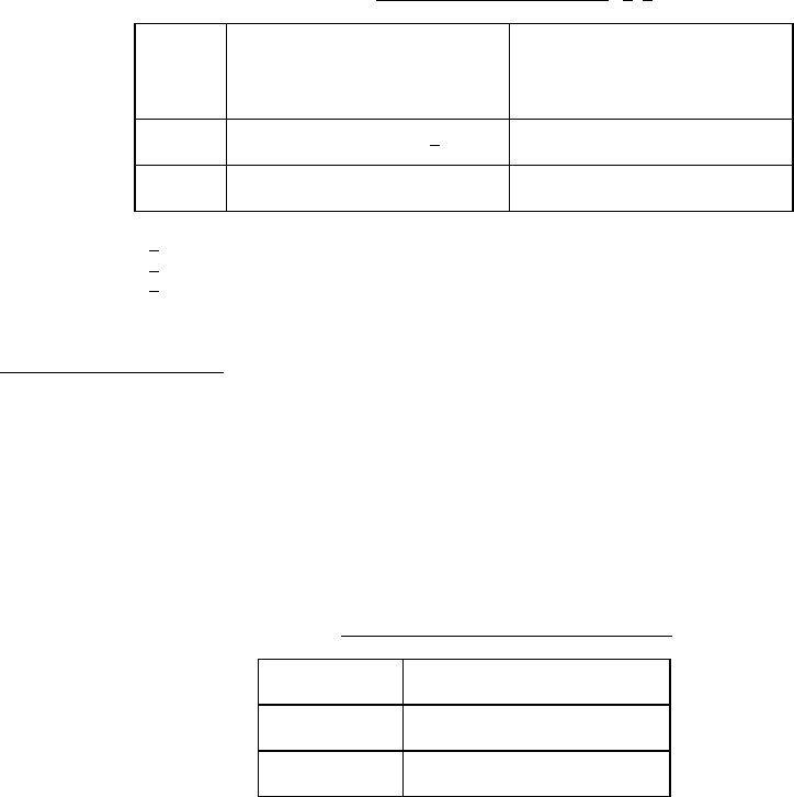
TABLE II. Pin combinations to be tested
. 1/ 2/
Terminal A
(Each pin individually
connected to terminal A
with the other floating)
Terminal B
(The common combination
of all like-named pins
connected to terminal B)
1. All pins except V
ps1
3/ All V
ps1
pins
2. All input and output pins All other input-output pins
1
/ Table II is restated in narrative form in 3.4 below.
2
/ No connects are not to be tested.
3
/ Repeat pin combination 1 for each named power supply and for ground (e.g.,
where V
ps1
is V
DD
, V
CC
, V
SS
, V
BB
, GND, +V
S
, -V
S
, V
REF
, etc.)
3.4 Pin combination to be tested
.
a. Each pin individually connected to terminal A with respect to the device ground pin(s) connected to terminal B. All pins
except the one being tested and the ground pin(s) shall be open.
b. Each pin individually connected to terminal A with respect to each different set of a combination of all named power
supply pins (e.g., V
SS1
or V
SS2
or V
SS3
or V
CC1
or V
CC2
) connected to terminal B. All pins except the one being tested and
the power supply pin or set of pins shall be open.
c. Each input and each output individually connected to terminal A with respect to a combination of all the other input and
output pins connected to terminal B. All pins except the input or output pin being tested and the combination of all the
other input and output pins shall be open.
TABLE III. Device ESD failure threshold classification
.
Class 1
0 volt to 1,999 volts
Class 2 2,000 volts to 3,999 volts
Class 3 4,000 volts and above

MIL-STD-883F
METHOD 3015.7
22 March 1989
4
4. SUMMARY. The following details shall be specified in the applicable purchase order or contract, if other than specified
herein.
a. Post test electricals.
b. Special additional or substitute pin combinations, if applicable.
c. Sample size, if other than three devices.
MIL-STD-883F
METHOD 3015.7
22 March 1989
5
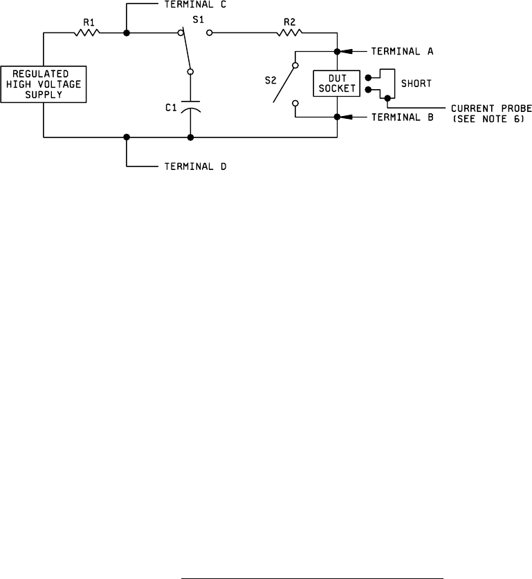
R1 = 10
6
ohms to 10
7
ohms
C1 = 100 picofarads ±10 percent (Insulation resistance 10
12
ohms minimum)
R2 = 1,500 ohms ±1 percent
S1 = High voltage relay (Bounceless, mercury wetted, or equivalent)
S2 = Normally closed switch (Open during discharge pulse and capacitance measurement)
NOTES:
1. The performance of this simulator circuit is strongly influenced by parasitics. Capacitances across relays and
resistor terminals, and series inductance in wiring and in all components shall be minimized.
2. As a precaution against transients upon recharge of C1, the supply voltage V
S
may be reduced before switch
S1 is returned to the charging position.
3. Piggybacking DUT sockets is not permitted during verification or classification testing.
4. Switching terminals A and B internal to the simulator to obtain opposite polarity is not recommended.
5. C1 represents the effective capacitance (see 2.3.2).
6. The current probe connection shall be made with double shielded cable into a 50-ohm termination at the
oscilloscope. The cable length shall not exceed 3 feet.
FIGURE 3015-1. EDS classification test circuit (human body model)
.